Featured Member

Event Coverage
ECTC 2024 3D InCites Community Member Preview
IMAPS DPC 2024 Community Member Preview
Upcoming Events
Job Openings
Top Stories
IFTLE 593: Deep in the Heart of Texas
Novel Surface Metrology Techniques for Hybrid Bonding
Will AI be Powered by Renewables? Maybe, But Not for Long
Sustainability 101: Rethinking Sustainable Materials
How Advanced Lithography Evolution Will Impact 3D Packaging
The Nexus of Innovation for U.S. Semiconductor Manufacturing


Trending Topic
#lithography · #wafer bonding 
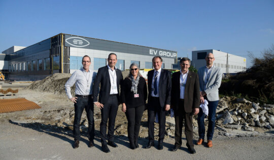
10 Years of Invent, Innovate, Implement at EV Group
Of all the companies that have supported 3DInCites over the past 10 years, none has been more consistently involved, both...
Volumes Matter and Other Conversations from SEMICON West 2018
The world wants intelligence in everything, especially things that aren’t nailed down like autonomous cars, and the internet of things...
Executive Viewpoint: Lithography’s Rising Star in the Year of the Fan-Out Package
There is no doubt about it, 2016 is turning out to be the year of fan-out wafer level packaging (FOWLP)...
Semiconductor Supplier Updates from SEMICON West 2015
No SEMICON West would be complete without a few laps around Moscone North and South, and some one-on-one chats with...
Wafer-to-Wafer Bonding Cost Analysis
Last year, I did an analysis that included the topic of wafer-to-wafer bonding. Specifically, it was a comparison of the...
Riding Out on a Horse and in on a Goat: 3D IC Predictions for MEMS
The Lunar New Year is soon upon us, and we will be celebrating the Year of the Goat with firecrackers,...
Lithography Challenges for 2.5D Interposer Manufacturing
In recent years, 2.5D packaging has quickly gained acceptance as an advanced packaging process, and the first products using this...
Lithography Process Innovations for 2.5/3D Part 1: Alleviating TSV Stress
As traditional semiconductor scaling becomes increasingly complex and cost-prohibitive, transitioning from planar chip packaging architectures to 2.5D/3D stacked die package...
Market Outlook for Permanent Wafer Bonding
Permanent wafer bonding can be categorized based on bonding with or without an intermediate layer. Intermediate layers can be subcategorized...
Europe in 3D: The EV Group Story Continues…
Rarely do I have the opportunity to visit a company two times and find something new to write about, never mind...
10 Years of Invent, Innovate, Implement at EV Group
Of all the companies that have supported 3DInCites over the past 10 years, none has been more consistently involved, both...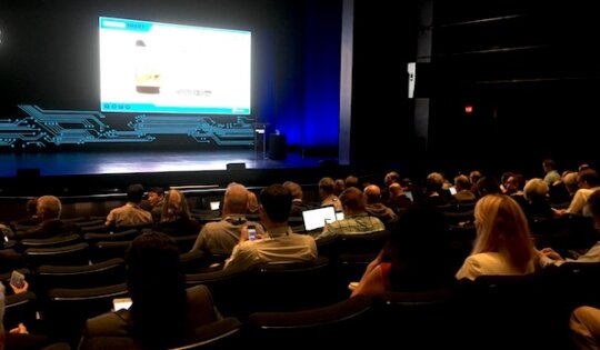
Volumes Matter and Other Conversations from SEMICON West 2018
The world wants intelligence in everything, especially things that aren’t nailed down like autonomous cars, and the internet of things...
Executive Viewpoint: Lithography’s Rising Star in the Year of the Fan-Out Package
There is no doubt about it, 2016 is turning out to be the year of fan-out wafer level packaging (FOWLP)...
Semiconductor Supplier Updates from SEMICON West 2015
No SEMICON West would be complete without a few laps around Moscone North and South, and some one-on-one chats with...
Wafer-to-Wafer Bonding Cost Analysis
Last year, I did an analysis that included the topic of wafer-to-wafer bonding. Specifically, it was a comparison of the...
Riding Out on a Horse and in on a Goat: 3D IC Predictions for MEMS
The Lunar New Year is soon upon us, and we will be celebrating the Year of the Goat with firecrackers,...
Lithography Challenges for 2.5D Interposer Manufacturing
In recent years, 2.5D packaging has quickly gained acceptance as an advanced packaging process, and the first products using this...
Lithography Process Innovations for 2.5/3D Part 1: Alleviating TSV Stress
As traditional semiconductor scaling becomes increasingly complex and cost-prohibitive, transitioning from planar chip packaging architectures to 2.5D/3D stacked die package...
Market Outlook for Permanent Wafer Bonding
Permanent wafer bonding can be categorized based on bonding with or without an intermediate layer. Intermediate layers can be subcategorized...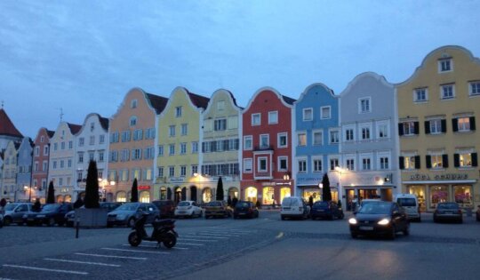
Europe in 3D: The EV Group Story Continues…
Rarely do I have the opportunity to visit a company two times and find something new to write about, never mind...Community Members