BRUKER KOREA Co., Ltd.

Seoul,  Korea (South)
http://www.bruker.com/nano
  • Booth: P118

Innovation with Integrity - Bruker

Overview

Founded in 1960, BRUKER in Germany is a global leader in the field of advanced analysis equipment and provides cutting-edge technologies and innovative analysis solutions. Bruker Nano Surfaces and Metrology(BNSM) division provides industry-leading surface analysis instruments for research and production. Our broad range of 2D and 3D surface profiler solutions supply the specific information needed to answer R&D, QA/QC, and surface measurement questions with speed, accuracy, and ease. Whatever your surface measurement and surface analysis needs, whatever your material or scale of investigation, BNSM has a specialized high-performance solution for you.


  Products

  • Dimension Nexus AFM and Dimension IconIR
    Nanoscale Infrared Spectrometer - Dimension IconIR : Photothermal AFM-IR for ultimate versatility in materials research and industrial R&D. Dimension Nexus AFM : Intersection of high performance and unbeatable value....

  • Bruker’s large-sample Dimension IconIR™ system combines nanoscale infrared (IR) spectroscopy and scanning probe microscopy (SPM) on one platform to deliver the most advanced spectroscopy, imaging, and property mapping capabilities available for academic researchers and industrial users. Incorporating decades of research and technological innovation, IconIR provides unrivaled performance based on and building off the industry-best AFM measurement capabilities of the Dimension Icon®. The system enables correlative microscopy and chemical imaging with enhanced resolution and monolayer sensitivity, while its unique large-sample architecture provides ultimate sample flexibility for the broadest range of applications. For example, the new IconIR polymer solution is an all-in-one package designed to include everything one would need to address key polymer research needs. The Dimension IconIR platform has the highest performance in the world for AFM-IR measurements, leveraging advancements in IR laser sources, system designs, and operating modes.

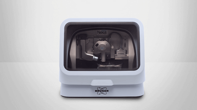
    Dimension Nexus™ delivers an ideal combination of data quality, experiment flexibility, and ease of use in a small-footprint system. It incorporates the milestone innovations of Bruker's NanoScope® 6 controller and PeakForce Tapping® technology to deliver more functionality than competing systems in its class. Suitable for both routine and custom experiments and easily upgradable in the field, Dimension Nexus is both an excellent starter system and a perfect addition to any thriving AFM lab.

  • Stylus Profilometer - Dektak Pro
    Proven technology, enhanced performance...

  • Building on 55 years of surface measurement innovation and technology leadership, Dektak Pro™ sets a new standard for stylus profilometer performance. The system uniquely delivers the highest quality data with unrivaled ease of use.

    This 11th-generation Dektak® system combines:

    • Unmatched accuracy and better than 4 Å repeatability
    • Accelerated measurement and analysis speed
    • A suite of Bruker-exclusive versatility and ease-of-use features
       

    Only Dektak Pro provides the latest stylus profilometry advances and reliability needed to support your cutting-edge research and industrial applications well into the future.

  • Hysitron TI 990 TriboIndenter
    Nanomechanical Test System : The world’s most comprehensive nanomechanical testing with unmatched performance...

  • Bruker's next-generation Hysitron TI 990 TriboIndenter® sets new standards for performance, flexibility, and usability in nanomechanical and nanotribological characterization. A comprehensive advancement of Bruker’s industry-leading TriboIndenter platform, every aspect of TI 990's measurement and analysis process features updated technologies designed to remove the normal limitations of nanoindenter systems. As such, this system features the most measurement modes available and delivers high-precision measurements in the broadest range of laboratory environments.
  • Automated AFM Metrology - InSight AFP
    Inline Metrology. Preferred Choice of Leading Foundries and Memory Makers...

  • InSight AFP is the world’s highest performance and industry preferred CMP profiling and etch depth metrology system for advanced technology nodes. The combination of its modern tip scanner with inherently stable capacitive gauges and an accurate air-bearing positioning system enables non-destructive, direct measurements in the active area of dies.

  • X-Ray Defect Inspection - JVSENSUS-600F
    X-ray diffraction imaging (XRDI) inspection system...

  • The JVSensus-600F is the X-ray defect metrology system for 300mm Si device manufacturers. It helps identify problems encountered during wafer production using the latest X-ray diffraction imaging (XRDI) technology. Applications include monitoring edge damage to prevent costly wafer breakage during ultra fast anneal. It can qualify and monitor process tools at any technology node, which reduces cycle times and facilitates fab expansion.

  • X-Ray Defect Inspection - X200
    High-resolution automated in-line X-ray inspection system...

  • The X200 X-ray Imaging (XRI) system is on the leading edge of a new category of in-line transmissive inspection and metrology equipment. This one-of-a-kind, no-compromises platform for advanced packaging provides fully automatic 100% inspection and real-time feedback on the die-attach process.

    As such, the high-speed, high-resolution X200 is the ideal defect inspection and production metrology solution for a wide range of semiconductor applications, from system-in-package (SiP) to 2.5D/3D integrated circuit (IC) integration.