Loading...

DR Laser Singapore Pte Ltd

Singapore,  Singapore 
Singapore
http://www.drlaser.com.cn/en
  • Booth: 1629

High-Precision Laser Equipment Provider for Manufacturing

Overview

DR Laser 

Define. Resolution. 

Our story of DR Laser begins in 2008 as a technology-based company aspiring to explore the frontiers of advanced laser applications. Amidst various opportunities, we chose to commit towards accelerating the commercialisation of solar cells, at a time when renewable energies and sustainability was not yet conventional. 

This decision proved to be correct. By 2017, we have delivered over 1000 machines with key laser technologies to the Photovoltatics industry. The advent of laser technologies has replaced old mechanical manufacturing methods, and made way for significant reduction in production costs in making solar panels; this allowed solar energy to become viable and affordable at scale. 

Having experienced our first success, DR Laser became a public listed company by 2019. We have built ourselves a corporation with 2,000 employees worldwide, that is generating more than USD200million dollars in yearly revenue. To date, we have installed more than 7000 machines globally, and our equipment are employed to achieve the existing world record for photovoltaic solar cell conversion efficiency. We have manufacturing capabilities in China and Singapore, having successfully shipped more than 1700 sets of equipment in the single year of 2023. Our R&D centers are located across China, Singapore, and Israel; with emphasis on the manufacturing industries of Photovoltaics, Advanced Displays and Semiconductor industry.

Today, we continue to serve the industry's leading companies by working closely to develop next-generation manufacturing processes. As DR Laser continues our quest towards engaging global customers in search of revolutionary technology - we are inviting you to join us on the next big thing. 


  Products

  • Cleave I-200 (Laser-induced Wafer Dicing)
    Wafer Dicing Solution: Cleave I- 200 is a laser-based dry process equipment to create internal cuts within wafer. When followed by a wafer breaker device, the result of separating a wafer into many individual dies is achieved.
    ...

  • The Cleave I- 200 is a dry process equipment which uses Laser to create a network of precise cuts at the wafer sub-surface level. When used in tandem with a wafer breaker device, the result of separating a wafer into many individual chips is achieved. The advantages of material processing at subsurface level are many. This technique allows narrow kerf and street width to be made - leading to increased wafer utilization. Since no material loss occurs in the process, there is also lower risk of contamination. Our system is fine-tuned based on silicon carbide wafer substrate, to produce thin chips with reduced heat affected zone and low mechanical stress, leading to good quality products and high yield rate.
  • Through-Glass Via (TGV) Microfabrication
    This product creates through-holes in glass substrates at high throughput. Based on subtractive fabrication technique consisting of two-steps: 1) Ultrafast laser modification; 2) Subsequent accelerated chemical etching....

  • This equipment utilizes Laser Accelerated Controlled Etching (LACE) technology to create large numbers of through-holes on glass substrates, that will undergo coating and metallization to achieve electrical conductivity between the top and bottom layers, which can be used in semiconductor and electronics packaging.


    LACE is a subtractive fabrication technique which consists of two-steps: laser modification, followed by chemical etching. During modification process, ultrafast laser is employed to induce phase changes in selective regions of the glass material. In subsequent chemical etching process, these phase-changed regions exhibit high etching efficiencies which leads to the formation of through-holes.

  • Pattern Transfer Printing (PTP™) system
    Laser-based method for transferring material.

    Features:
    Non-contact printing of paste/slurry
    High resolution
    High aspect-ratio...

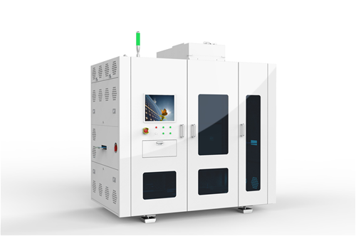
  • DR Laser has acquired the patent of Israel-based research centre, Utilight, to create the world’s first - Pattern Transfer Printing (PTP™) system.

    This equipment is created to precisely deposit microscopic silver lines onto solar cells, in a process known as “metallization”.

    The PTP™ works by filling silver paste into a patented-design, trench-shaped, organic polymer carrier tape. The process is followed by the alignment and scanning of a high-power laser beam upon the trenches, which completes the material transfer of silver paste from the carrier tape onto the surface of battery cell.

    Our method has achieved an all-around improvement in the transfer printing of metal gridlines for battery cells. In comparison with conventional methods, the PTP™ technology is a contactless process which enables narrower linewidths and better aspect ratios, enhancing the efficiency of the solar cell, reducing slurry consumption, and lowering the production cost of the battery cell.

    In today’s industry, metallization
    line integration, and as a standalone equipment.  

For Technical Support with this webpage, please contact support.