[March 6, 2025 – Singapore] Test Research, Inc. (TRI), the leading test and inspection systems provider for the electronics manufacturing industry, will join SEMICON SEA held at the SANDS Expo and Convention Centre in Singapore from May 20 - 22, 2025. Visit booth #L2632 to learn about AI-powered AOI solutions for Advanced WLP/PLP and SEMI Back-End Package processes.
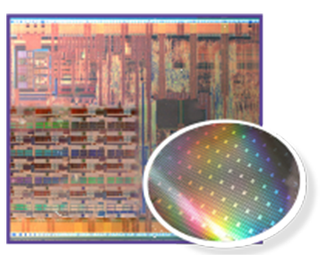
TRI will be exhibiting the new Wafer Inspection Platform, TR7950Q SII, featuring a High-resolution 2.5 μm 25MP camera and the TSV Metrology Module. The TR7950Q SII can perform Wafer Macroscopic 3D Inspection and micro measurement metrology. The TR7950Q SII can inspect Advanced WLP, Wafer Frame, Patterned Wafer, Wafer Bumping, WLCSP, through-silicon via (TSV), and more. The TR7950Q SII can measure TSV at ultra-high speeds, measuring sensing TSV depth, trench depth, oxide, nitride, PR, and PI film thickness.
| 
Patterned Wafer | 
TSV Metrology | 
Wafer Frame | 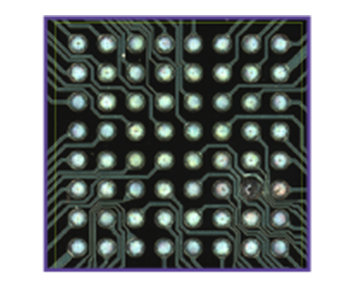
Wafer Bumping | 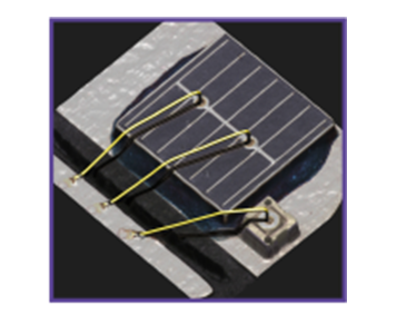
Wire/Die |
Additionally, TRI will showcase the TR7007Q SII-S, the high-accuracy 3D SEMI SPI for precise solder measurements, supporting applications such as Mini-LED, C4 bumps (~100 μm Ø), and 008004 paste inspection. The lineup will also feature an X-ray Inspection Demo Station.
Join us at SEMICON SEA 2025 (booth #L2632) to discover TRI's cutting-edge SEMI inspection and metrology solutions!
###
About TRI
TRI offers the most robust product portfolio in the industry for Automatic Test and Inspection solutions. From Optical Inspection to Board Testing, TRI provides the most cost-effective solutions to meet a comprehensive range of manufacturing Test and Inspection requirements. Learn more at http://www.tri.com.tw. For sales and service information, please write to us at [email protected] or call +604 6461171.