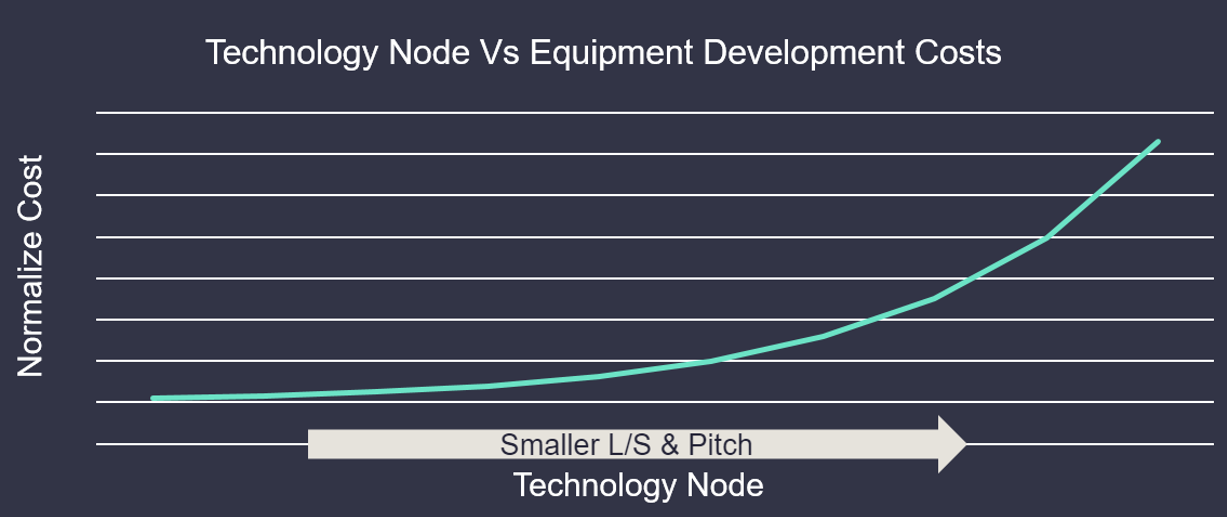
The accelerating costs of transistor scaling are pushing the industry to find innovative ways to improve chip and system performance from generation to generation. That’s why heterogenous integration (HI) has become the latest inflection in packaging technology.
-
Heterogeneous integration (HI) brings together (integrates) separately manufactured components into a higher-level assembly that, in aggregate, provides enhanced functionality and improved operating characteristics and lower cost.
-
This higher-level assembly is called System in Package (SiP).
-
HI is initially being implemented on high performance computing devices often used in machine learning and artificial intelligence applications.
SiP Designs
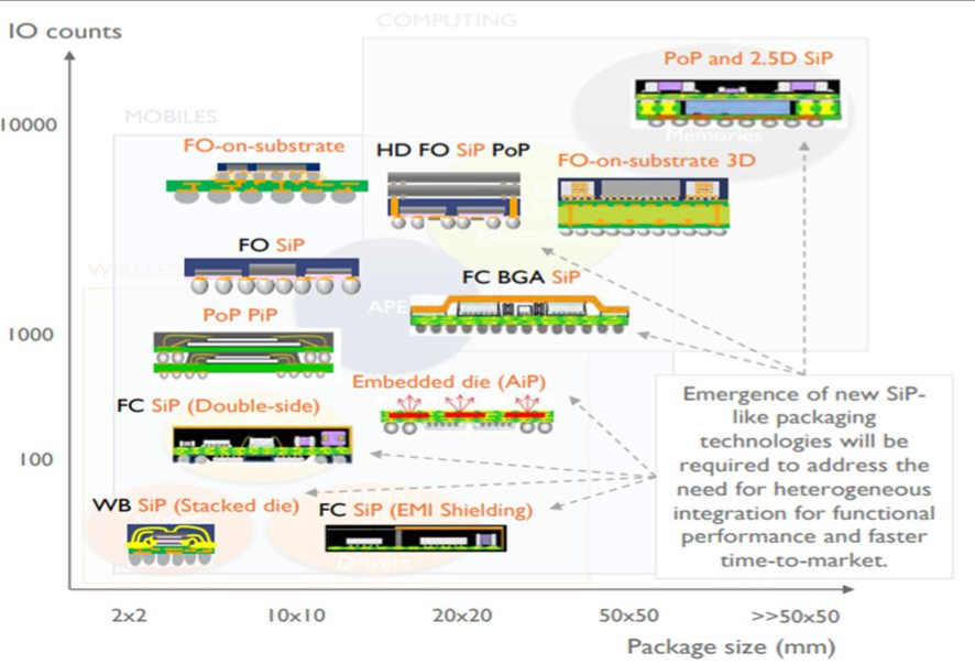
Increasing performance is about bringing logic and memory closer together with higher bandwidth connections than can be achieved with individual chips mounted to a mother board. To increase speed and bandwidth the industry is embracing System in Package (SiP) designs.
-
SiP is a is a way of bundling two or more integrated circuits (ICs) inside a single package. Contrast this with system on a chip (SoC), where the functions on those chips are integrated onto the same die.
-
SiP designs continue to evolve to include more functionality as close together as possible.
-
Some of the most advanced devices today have dozens of chips in a single package with transistor counts exceeding one trillion(!).

To bring logic and memory closer together, the industry is moving SiP designs to an integrated circuit (IC) substrate, which provides smaller features, tighter pitches, and higher I/O (input/output) counts than can be achieved on a standard PCB (printed circuit board).
These factors push the design rules on a substrate to be more like that of Wafer Level Fanout (FO-WLP) and Panel Level Fan Out (FO-PLP).
-
Fan Out is an emerging technique where chips are attached to larger format substrates that could be round, square, or rectangular. The use of large format enables more chips per area, resulting in lower per unit costs.
-
FO-PLP provides cost benefits over FOWLP, which creates the package in a round 300/330 mm format.
But increasing costs for R&D of FO-PLP technology at low volumes is an immense obstacle.
R&D Challenges

The primary driver in the FO-PLP market is cost (not performance). The challenge for this market is to be able to meet wafer level specifications and yields on a larger format, going from 300mm round wafers to 600X600mm square panels.
The market for these panels is small. Consequently, there is not enough volume to allow a high enough level of R&D investment across the entire supply chain to solve key issues associated with processing large panels.
The result? Most fanout business stays on wafers.
Technical Convergence
Similar panels (510X515mm) are used in the substrate market, where we expect to see a significant increase in volume over the next four years, especially in the most technologically challenging segments.
Since technical convergence for substrate and FO-PLP requirements (e.g., feature size, uniformity) is imminent, it’s likely we could use the same or similar platforms to address both markets. The convergence enables a stronger equipment supplier base—a cause for hope.
By standardizing panels to a few sizes and adopting existing interface and equipment standards, we can increase volumes for a common system platform. Standardization will help decrease R&D costs for panel level processing systems.
As panel yields approach those seen in wafer level packaging, we would expect to see movement of additional applications from wafers to panels to take advantage of the expected cost benefit.

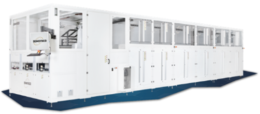
Semsysco offers wet processing tools (like CUPID. above). It is capable of processing up to 600x600mm size substrate.
Domino Effect
As yields improve, we believe a domino effect will take place with reduced costs driving more volume and more R&D investment. These investments will help drive more effective automation, additional machine learning and intelligence, higher reliability, and lower defects.
Lam has always contributed to the extraordinary pace of innovation in the semiconductor industry. With the recent acquisition of Semsysco, we are investing in the panel level processing market and keeping Lam at the forefront of innovation.