Loading...

Lam Research

Salzburg,  Austria
https://www.lamresearch.com/
  • Booth: M0958

Please visit Lam Research at M0958 in Semicon Taiwan 2024.

Overview

COMPANY OVERVIEW

From smartphones and tablets to wearables and automobiles, it’s hard to go more than a few hours without using a semiconductor-enabled device. The semiconductor industry touches nearly every person on the planet, and chipmakers continue to advance the technology that powers it all. As a trusted partner to the world’s leading semiconductor companies, we welcome challenges and we deliver. That’s why, today, nearly every advanced chip is built with Lam technology. Our innovative wafer fabrication equipment and services allow chipmakers to build smaller and better performing devices. We combine superior systems engineering, technology leadership, and a strong values-based culture, with an unwavering commitment to our customers. 


  Press Releases

    • System in Package (SiP) needs push substrate designs to smaller features (similar to FO-PLP)   

    • Convergence in requirements allows shared R&D costs for panel level processing systems 

    The accelerating costs of transistor scaling are pushing the industry to find innovative ways to improve chip and system performance from generation to generation. That’s why heterogenous integration (HI) has become the latest inflection in packaging technology.  

    • Heterogeneous integration (HI) brings together (integrates) separately manufactured components into a higher-level assembly that, in aggregate, provides enhanced functionality and improved operating characteristics and lower cost. 

    • This higher-level assembly is called System in Package (SiP).   

    • HI is initially being implemented on high performance computing devices often used in machine learning and artificial intelligence applications.  

    SiP Designs 

    Increasing performance is about bringing logic and memory closer together with higher bandwidth connections than can be achieved with individual chips mounted to a mother board. To increase speed and bandwidth the industry is embracing System in Package (SiP) designs.  

    • SiP is a is a way of bundling two or more integrated circuits (ICs) inside a single package. Contrast this with system on a chip (SoC), where the functions on those chips are integrated onto the same die.

    • SiP designs continue to evolve to include more functionality as close together as possible.  

    • Some of the most advanced devices today have dozens of chips in a single package with transistor counts exceeding one trillion(!).  

    The chart shows options for System in Package designs. The chart says, Emergence of new SiP-like packaging technologies will be required to address the need for heterogeneous integration for functional performance and faster time-to-market.

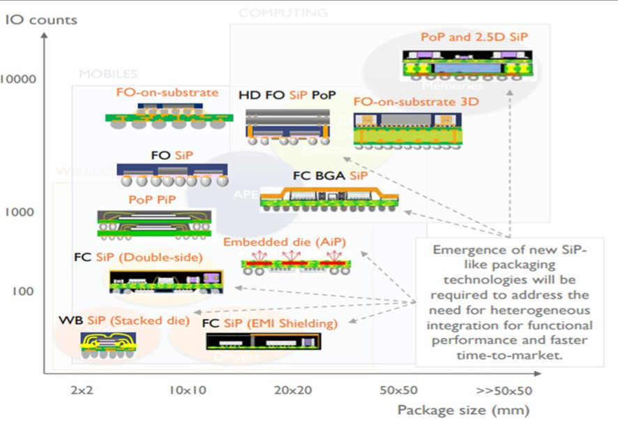
    To bring logic and memory closer together, the industry is moving SiP designs to an integrated circuit (IC) substrate, which provides smaller features, tighter pitches, and higher I/O (input/output) counts than can be achieved on a standard PCB (printed circuit board).  

    These factors push the design rules on a substrate to be more like that of Wafer Level Fanout (FO-WLP) and Panel Level Fan Out (FO-PLP). 

    • Fan Out is an emerging technique where chips are attached to larger format substrates that could be round, square, or rectangular. The use of large format enables more chips per area, resulting in lower per unit costs.  

    • FO-PLP provides cost benefits over FOWLP, which creates the package in a round 300/330 mm format. 

    But increasing costs for R&D of FO-PLP technology at low volumes is an immense obstacle. 

    R&D Challenges 

    A chart showing how costs increase as technology nodes decrease in size

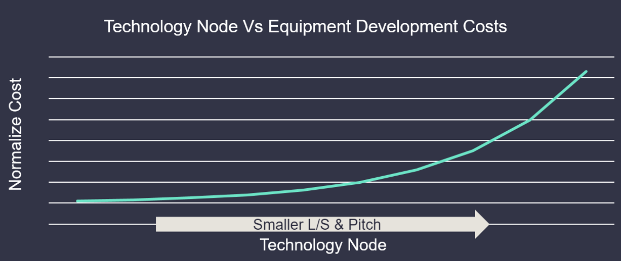
    The primary driver in the FO-PLP market is cost (not performance). The challenge for this market is to be able to meet wafer level specifications and yields on a larger format, going from 300mm round wafers to 600X600mm square panels.  

    The market for these panels is small. Consequently, there is not enough volume to allow a high enough level of R&D investment across the entire supply chain to solve key issues associated with processing large panels.  

    • Due to under-investment the yields for FO-PLP have not reached the levels needed to obtain the economic benefits of going to a larger substrate size.  

    The result? Most fanout business stays on wafers.   

    Technical Convergence 

    Similar panels (510X515mm) are used in the substrate market, where we expect to see a significant increase in volume over the next four years, especially in the most technologically challenging segments. 

    Since technical convergence for substrate and FO-PLP requirements (e.g., feature size, uniformity) is imminent, it’s likely we could use the same or similar platforms to address both markets. The convergence enables a stronger equipment supplier base—a cause for hope.  

    By standardizing panels to a few sizes and adopting existing interface and equipment standards, we can increase volumes for a common system platform. Standardization will help decrease R&D costs for panel level processing systems.  

    • Increased volumes will facilitate spreading the costs across additional equipment. This could create the scale needed to enable a robust market for panel processing equipment.  

    As panel yields approach those seen in wafer level packaging, we would expect to see movement of additional applications from wafers to panels to take advantage of the expected cost benefit. 

    • Adjacent markets like micro-LEDs or “antenna in package” solutions are also expected to drive panel volumes higher. These additional volumes can improve the opportunities to reduce costs to help increase competitiveness of panel level solutions.  

    Semsysco’s CUPID wet processing tool

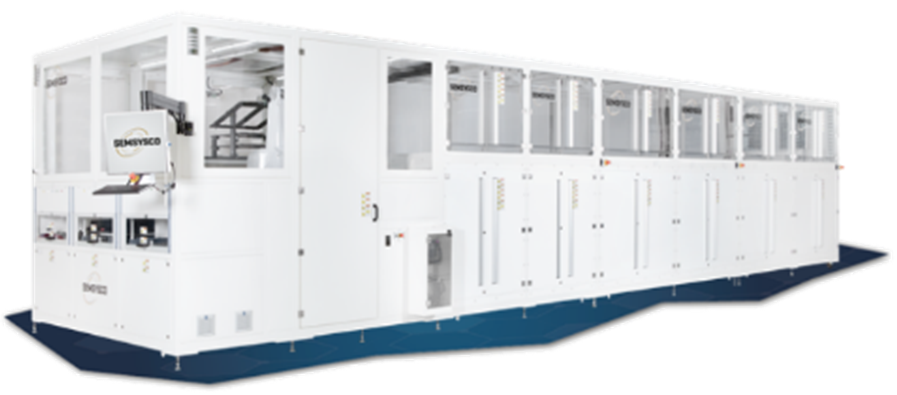
    Semsysco offers wet processing tools (like CUPID. above). It is capable of processing up to 600x600mm size substrate.  

    Domino Effect  

    As yields improve, we believe a domino effect will take place with reduced costs driving more volume and more R&D investment. These investments will help drive more effective automation, additional machine learning and intelligence, higher reliability, and lower defects.  

    • All of this should result in lower costs, which should continue to drive more volume to the panel business.  

    Lam has always contributed to the extraordinary pace of innovation in the semiconductor industry. With the recent acquisition of Semsysco, we are investing in the panel level processing market and keeping Lam at the forefront of innovation.  

    John Ostrowski is the managing director for Lam’s Sabre 3D product line. Drivers focuses on the macroeconomic and industry trends driving demand for semiconductors. Chip photo by Bermix Studio on Unsplash.

    Heterogeneous Integration Drives an Inflection in Panel Processing Equipment (lamresearch.com)

  • Enabling the future of panel processing

    Panel Processing is expected to enable the continuation of scaling in the semiconductor industry. The movement to chiplets and Heterogeneous Integration to create the next generation of semiconductor products is part of the future of the industry. Lam brings the capability and quality of wafer scale processing to the panel market. This includes the continued scaling in the substrate market, the expansion of the PLP market to the promise of the microLED display technology. Lam can provide the technology and equipment required for these markets.

    This includes the plating, wet strip, clean and etch processes. Our systems and technology covers many steps within each of the panel processing markets including: RDL, Pads, FLI, Cu Pillar, Cu Buildup, and TGV layers. Lam’s panel process equipment provides the precision, performance, and flexibility needed for a wide range of challenging device applications.

    Panel Processing - Lam Research


  Products

  • Kallisto Product Family
    Electrochemical Deposition (ECD)

    Advanced Memory, Advanced Packaging, Advanced Substrates, Analog & Mixed Signal, Automotive, Discrete & Power Devices, Mini/Micro LED, Optoelectronics & Photonics, Panel Level Fanout...

  • An advanced vertical processing platform for wet chemical treatment of substrates from 300x300mm up to Gen 5.1 (1100 x 1300mm) tailored to the needs of semi industry.

    Inspired by wafer level performance Kallisto offers a broad range of processing capabilities to address the future market requirements driven by AI, high performance computing and other applications.

    Kallisto enables fine line plating on structures <10µm on various materials including organic and glass core technologies.

    Processing can be single or dual sided depending on the application.

    Industry Challenges

    Advanced packaging is becoming an increasingly critical approach to continue scaling beyond silicon. Several device manufacturers and fabless companies are increasing adoption of novel chiplet solutions to meet performance and cost requirements. This accelerating chiplet transition requires new packaging solutions and innovations in the substrate market segment. As traditional silicon scaling approaches cost and technology limitations, companies are adopting novel chiplet and heterogenous integration solutions. To ensure continued scaling, substrate solutions require several innovations in process equipment solutions. In addition to meeting the technology roadmap needs, substrate level equipment must have increased flexibility to process panels of various materials and sizes. In addition, high productivity and low cost of ownership are desirable for high volume manufacturing environments.

    Key Customer Benefits

    • Semi- and fully-automated systems
    • Processing of 300x300mm up to 1100x1300mm (Gen5.1) substrates
    • Thin glass handling capability down to 200um
    • Simultaneous double sided processing of panels
    • Full exposed panel surface treatment due to vacuum chuck technology
    • Plating uniformity performance
    • Ready for online dosing and chemical monitoring system (internal/external)
    • Flexible Tool layouts tailored to fab environment - optimized for low cost of ownership
    • https://www.lamresearch.com/product/kallisto-product-family/
  • Phoenix Product Family
    Electrochemical Deposition (ECD) PR-Development PR-Strip Wet Clean/Strip

    Advanced Memory, Advanced Packaging, Advanced Substrates, Analog & Mixed Signal, Automotive, Discrete & Power Devices, Mini/Micro LED, Optoelectronics & Photonics, Panel Level Fanout...

  • Phoenix offers a fully-automated high volume panel processing for 510x515mm substrates.

    Designed with the goal to redefine cost of ownership, Phoenix delivers unique technologies in the panel level packaging industry together with a respectful usage of its operating utilities.

    Inspired by wafer level performance Phoenix offers strip, development, etch and plating solutions to address the future market requirements driven by AI, high performance computing and other applications.

    Industry Challenges

    Advanced packaging is becoming an increasingly critical approach to continue scaling beyond silicon. Several device manufacturers and fabless companies are increasing adoption of novel chiplet solutions to meet level performance and cost requirements. This accelerating chiplet transition requires new packaging solutions and innovations in the substrate market segment. As traditional silicon scaling approaches cost and technology limitations, companies are adopting novel chiplet and heterogenous integration solutions. To ensure continued scaling, substrate solutions require several innovations in process equipment solutions. In addition to meeting the technology roadmap needs, substrate level equipment must have increased flexibility to process panels of various materials and sizes. In addition, high productivity and low cost of ownership are desirable for high volume manufacturing environments.

    Key Customer Benefits

    • Fully automated system for large volume
    • Processing of 510x515mm panels
    • Thin glass handling capability
    • Simultaneous double sided treatment of panels
    • Full exposed panel surface treatment due to vacuum chuck technology
    • Plating and etch uniformity performance
    • Ready for online dosing and chemical monitoring system (internal/external)
    • Flexible Tool layouts tailored to fab environment - optimized for low cost of ownership
    • https://www.lamresearch.com/product/phoenix-product-family/
  • Triton Product Family
    Electrochemical Deposition (ECD) Wet Clean/Strip

    Advanced Memory, Advanced Packaging, Analog & Mixed Signal, Automotive, Discrete & Power Devices, Mini/Micro LED, Optoelectronics & Photonics...

  • The Triton platform is a versatile and modular solution for single wafer plating and wet processing. Its design makes this system the first choice for R&D and is expandable to support high volume production.

    The platform allows processing of acids and solvents in one system. This makes the Triton an ideal solution to address various process steps in the smallest space.

    Electrochemical deposition with patented plating technology enables superior uniformity and yield performance in line with the growing market demand of fine line plating.

    Industry Challenges

    Future advanced chip layouts require technologies supporting continuous shrinking of feature designs. While generating the interconnect layers, advanced plating solutions ensure a defect-free metallization.

    Continual thinning of the barrier/seed stack along with line width shrinkage requires increasingly stringent process control to achieve sufficient bottom-up fill rate while protecting the seed layer. The broad range of feature geometries in a single logic layer requires a wide process window to ensure proper filling of structures with large variations in aspect ratio, seed coverage, and density.

    Key Customer Benefits

    • Full modularity on minimal footprint – extendable platform to support increasing demand
    • Processing of 3” to 300 mm wafers, flat panel processing up to 300x300mm
    • Processing of different substrate sizes on one platform
    • Patented high speed plating technology
    • Plating and etch uniformity performance
    • End-point monitoring for highest product quality
    • Ready for online dosing and chemical monitoring system (internal / external)
    • Tool layouts customized to required process and fab environment
    • https://www.lamresearch.com/product/triton-product-family/