Featured Member

Event Coverage
SEMICON China 2024 Community Member Preview
SEMICON Europa 3D InCites Member Spotlight: What We’re Doing to Shape a Sustainable $1 Trillion Era
Upcoming Events
Job Openings
Top Stories
IFTLE 591: TSMC AZ & Samsung get CHIPS Money; IMAPS Hosts 2nd Annual Onshoring Conference
IFTLE 590: The NHanced Semiconductors Roadmap
Sustainability 101: Refuse, Reduce, Repair, Refurbish, Rework
Five Workflows for Tackling Heterogeneous Integration of Chiplets for 2.5D/3D
The Role of 200mm Manufacturing in Enabling a $1 Trillion Semiconductor Industry
Taking Stock of Global Investments in Semiconductor Manufacturing


Trending Topic
#wafer-level packaging View all

Advanced Packaging – Measuring Deep Etch Trenches
Adoption of advanced packaging is accelerating as the benefit of the classic Moore’s Law transistor shrink diminishes on a monolithic...
Wafer-Level Packaging Is Well-Positioned for Growth
Wafer-level packaging (WLP) saw significant growth in 2021 due in large part to the increased performance needs of data-driven 5G...
Trends in Semiconductor Manufacturing: Wafer-Level Packaging
One of the hottest trends in semiconductor manufacturing today is wafer-level packaging (WLP). According to Allied Market Research, the global...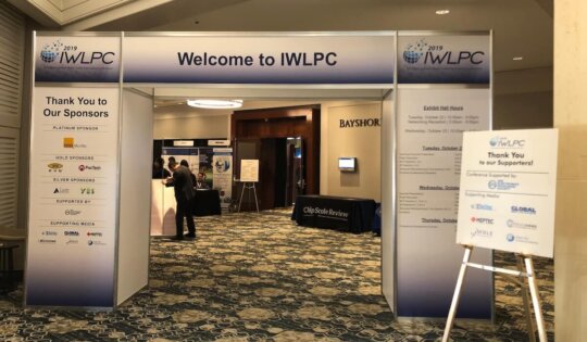
IWLPC 2019 Brings You Advanced Packaging in an Interconnected World
Anyone whose anyone with a hand in the evolution of wafer level packaging will be in attendance or exhibiting at...
Why Today’s Advanced Packages Need Better Inspection and What’s Being Done About It
It’s almost ironic. As CMOS scaling (aka: Moore’s Law) has slowed due to the increased complexity and cost of achieving...
The 14th 3D ASIP Conference Addresses a Spectrum of 0pportunities, Part 1
Several years before I started promoting 3D IC benefits in 2008, a small team of industry visionaries founded the 3D...
Pasadena offers Roses and Technology
California’s Pasadena is well known for the New Year Rose Parade and the Rose Bowl. There is no doubt: It...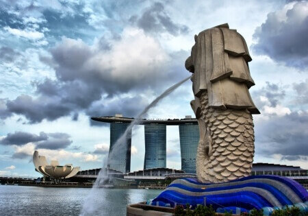
Wafer Level Packaging and Stacking take Center Stage at Asia Conferences
I thought I would go to Singapore, attend EPTC (Electronic Packaging Technology Conference 2013) and then take off on my...
How will the 450mm Transition Affect Advanced Packaging and 3D ICs?
That was my kick-off question for Manish Ranjan, Vice President, Product Marketing, Advanced Packaging/Nanotechnology Segment at Ultratech, during our annual...Talking 3D with Manish Ranjan
I’ll never forget the first time I interviewed Manish Ranjan of Ultratech. It was during my first SEMICON West experience...Community Members