Search Thermo Fisher Scientific

bf5a- Apps/Techniques/Products/Resources/Contact Us
Semiconductor metrology and analysis
To meet tomorrow’s performance and power efficiency needs, the semiconductor industry continues to innovate and push technology boundaries.

For more than four decades, semiconductor researchers, designers, and manufacturers have counted on Thermo Fisher Scientific to provide failure analysis, metrology, and characterization solutions.
Learn how Thermo Fisher Scientific is helping create tomorrow’s logic, memory, power, display devices, and more.

From research and development to high-volume manufacturing and beyond, Thermo Fisher Scientific offers a broad portfolio of solutions and workflows to support semiconductor development and accelerate time-to-market.

Scalable TEM lab automation
Streamline data collection between the lab and the fab. Learn how our integrated TEM metrology workflow is poised to revolutionize TEM lab automation.

Semiconductor Advanced Packaging
Performance, power efficiency, area, and cost are driving packaging innovations. Learn how workflows provide fast, precise, and accurate time-to-data.

Semiconductor Memory Devices
Data demands are driving 3D NAND, DRAM and other memory structure innovations. Learn how analysis tools and workflows offer accurate visibility of buried features and defects.

Semiconductor power devices
Novel architectures and materials pose new challenges. Learn how to pinpoint faults and characterize materials, structures, and interfaces.

Semiconductor research and development
Innovation starts with research and development. Learn more about solutions to help you understand innovative structures and materials at the atomic level.

Semiconductor materials characterization
Many factors impact yield, performance, and reliability. Learn more about solutions to characterize physical, structural, and chemical properties.

Semiconductor metrology
Manufacturing today’s complex semiconductors requires exact process controls. Learn more about advanced metrology and analysis solutions to accelerate yield learnings.

Semiconductor display technology
Display technologies are evolving to improve display quality and light conversion efficiency. Learn how metrology, failure analysis, and characterization solutions provide insights.

Chemical Structure and Composition Analysis
From incoming raw materials through fabrication and QA/QC, vibrational spectroscopy techniques provide detailed information about the chemical composition, molecular structure, and crystal orientation of the materials.

Ultra-High Purity Gas Analysis
Impure gas can lead to poor device performance, production delays and revenue loss. Learn how you can continuously measure bulk gases with more accurate analysis and lower detection limits than any other technologies.

Semiconductor Advanced Logic Transistor Analysis
Advanced logic manufacturers are introducing new metrology, defect analysis, and failure analysis challenges with the transition to gate-all-around transistor. Our industry-recognized solutions let you accurately root cause, measure, and characterize yield-limiting defects to accelerate yield learning cycles, improve production yield, and enhance device performance.

Semiconductor Failure Analysis
Complex semiconductor device structures result in more places for defects to hide. Learn more about failure analysis solutions to isolate, analyze, and repair defects.


Semiconductor Leaning Center
The content you will find contains information on new techniques and workflows to provide you with accurate and reliable insights and capabilities to assist in accelerating semiconductor design, analysis and production. Via the learning center you will be able to access application notes, videos, webinars, white papers and blogs.

SPARK Webinars
SPARK is a knowledge community where semiconductor professionals and industry thought leaders come together to share information on failure analysis, metrology and characterization techniques. Our webinars highlight the latest advances in semiconductor analysis, enabling you to stay at the forefront of an evolving technology and application landscape.

Illuminating Semiconductors
Semiconductor manufacturing stories and solutions about a more connected, more autonomous, and smarter world.
Videos
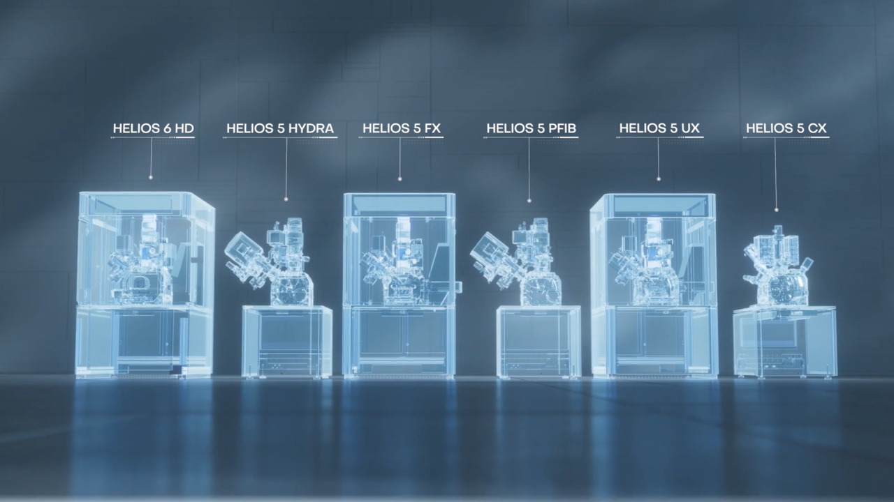
The Thermo Scientific Helios DualBeam Family
Style Sheet for Komodo Tabs


TEM Metrology
Advanced and automated TEM metrology routines deliver significantly greater precision than manual methods. This allows users to generate large amounts of statistically relevant data, with sub-angstrom-level specificity, that is free of operator bias.

Semiconductor TEM Imaging and Analysis
Thermo Scientific transmission electron microscopes offer high-resolution imaging and analysis of semiconductor devices, enabling manufacturers to calibrate toolsets, diagnose failure mechanisms, and optimize overall process yields.

Circuit Edit
Advanced, dedicated circuit edit and nanoprototyping solutions, which combine novel gas-delivery systems with a broad portfolio of chemistries and focused ion beam technology, offer unparalleled control and precision for semiconductor device development.

SEM Metrology
Scanning electron microscopy provides accurate and reliable metrology data at nanometer scales. Automated ultra-high-resolution SEM metrology enables faster time-to-yield and time-to-market for memory, logic, and data storage applications.

Semiconductor Analysis and Imaging
Thermo Fisher Scientific offers scanning electron microscopes for every function of a semiconductor lab, from general imaging tasks to advanced failure analysis techniques requiring precise voltage-contrast measurements.

Optical Fault Isolation
Increasingly complex designs complicate fault and defect isolation in semiconductor manufacturing. Optical fault isolation techniques allow you to analyze the performance of electrically active devices to locate critical defects that cause device failure.

Thermal Fault Isolation
Uneven distribution of local power dissipation can cause large, localized increases in temperature, leading to device failure. We offer unique solutions for thermal fault isolation with high-sensitivity lock-in infrared thermography (LIT).

Sample Preparation of Semiconductor Devices
Thermo Scientific DualBeam systems provide accurate TEM sample preparation for atomic-scale analysis of semiconductor devices. Automation and advanced machine learning technologies produce high-quality samples, at the correct location, and a low cost per sample.

Nanoprobing
As device complexity increases, so does the number of places defects have to hide. Nanoprobing provides the precise localization of electrical faults, which is critical for an effective transmission electron microscopy failure analysis workflow.

APT Sample Preparation
Atom probe tomography (APT) provides atomic-resolution 3D compositional analysis of materials. Focused ion beam (FIB) microscopy is an essential technique for high-quality, orientation, and site-specific sample preparation for APT characterization.

Semiconductor Laser Ablation
Laser ablation provides high-throughput milling of semiconductor devices for imaging and analysis with electron microscopy, while still preserving sample integrity. Access large-volume 3D data and optimize milling conditions to best suit your sample type.

Device Delayering
Shrinking feature size, along with advanced design and architecture, results in increasingly challenging failure analysis for semiconductors. Damage-free delayering of devices is a critical technique for the detection of buried electrical faults and failures.

ESD Compliance Testing
Electrostatic discharge (ESD) can damage small features and structures in semiconductors and integrated circuits. We offer a comprehensive suite of test equipment which verifies that your devices meet targeted ESD compliance standards.

Atmospheric Pressure Ionization Mass Spectrometry (API-MS)
Perform routine continuous measurement of contaminants including water and oxygen to single-digit ppt levels. These gas analyzers offer a cost effective alternative to conventional quality control techniques allowing each bulk gas to be monitored for a range of potential contaminants, while achieving lower detection limits (up to 100 times better) than any other technology.
TEM Metrology
Advanced and automated TEM metrology routines deliver significantly greater precision than manual methods. This allows users to generate large amounts of statistically relevant data, with sub-angstrom-level specificity, that is free of operator bias.
Semiconductor TEM Imaging and Analysis
Thermo Scientific transmission electron microscopes offer high-resolution imaging and analysis of semiconductor devices, enabling manufacturers to calibrate toolsets, diagnose failure mechanisms, and optimize overall process yields.
Circuit Edit
Advanced, dedicated circuit edit and nanoprototyping solutions, which combine novel gas-delivery systems with a broad portfolio of chemistries and focused ion beam technology, offer unparalleled control and precision for semiconductor device development.
SEM Metrology
Scanning electron microscopy provides accurate and reliable metrology data at nanometer scales. Automated ultra-high-resolution SEM metrology enables faster time-to-yield and time-to-market for memory, logic, and data storage applications.
Semiconductor Analysis and Imaging
Thermo Fisher Scientific offers scanning electron microscopes for every function of a semiconductor lab, from general imaging tasks to advanced failure analysis techniques requiring precise voltage-contrast measurements.
Optical Fault Isolation
Increasingly complex designs complicate fault and defect isolation in semiconductor manufacturing. Optical fault isolation techniques allow you to analyze the performance of electrically active devices to locate critical defects that cause device failure.
Thermal Fault Isolation
Uneven distribution of local power dissipation can cause large, localized increases in temperature, leading to device failure. We offer unique solutions for thermal fault isolation with high-sensitivity lock-in infrared thermography (LIT).
Sample Preparation of Semiconductor Devices
Thermo Scientific DualBeam systems provide accurate TEM sample preparation for atomic-scale analysis of semiconductor devices. Automation and advanced machine learning technologies produce high-quality samples, at the correct location, and a low cost per sample.
Nanoprobing
As device complexity increases, so does the number of places defects have to hide. Nanoprobing provides the precise localization of electrical faults, which is critical for an effective transmission electron microscopy failure analysis workflow.
APT Sample Preparation
Atom probe tomography (APT) provides atomic-resolution 3D compositional analysis of materials. Focused ion beam (FIB) microscopy is an essential technique for high-quality, orientation, and site-specific sample preparation for APT characterization.
Semiconductor Laser Ablation
Laser ablation provides high-throughput milling of semiconductor devices for imaging and analysis with electron microscopy, while still preserving sample integrity. Access large-volume 3D data and optimize milling conditions to best suit your sample type.
Device Delayering
Shrinking feature size, along with advanced design and architecture, results in increasingly challenging failure analysis for semiconductors. Damage-free delayering of devices is a critical technique for the detection of buried electrical faults and failures.
ESD Compliance Testing
Electrostatic discharge (ESD) can damage small features and structures in semiconductors and integrated circuits. We offer a comprehensive suite of test equipment which verifies that your devices meet targeted ESD compliance standards.
Atmospheric Pressure Ionization Mass Spectrometry (API-MS)
Perform routine continuous measurement of contaminants including water and oxygen to single-digit ppt levels. These gas analyzers offer a cost effective alternative to conventional quality control techniques allowing each bulk gas to be monitored for a range of potential contaminants, while achieving lower detection limits (up to 100 times better) than any other technology.


Style Sheet for Instrument Cards Original
Style Sheet to change H2 style to p with em-h2-header class
Style Sheet for Support and Service footer
Style Sheet for Fonts
Style Sheet for Cards
Electron microscopy services for
semiconductors
To ensure optimal system performance, we provide you access to a world-class network of field service experts, technical support, and certified spare parts.