PRESS RELEASE
December 4, 2025
High-precision wafer measurement meets surging demand from AI and data centers
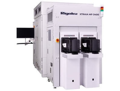 Rigaku Corporation, a global solution partner in X-ray analytical systems and a group company of Rigaku Holdings Corporation (headquarters: Akishima, Tokyo; CEO: Jun Kawakami; hereinafter “Rigaku”) has launched the XTRAIA MF-3400, an instrument used in semiconductor manufacturing processes to measure the thickness and composition of wafers. The XTRAIA MF-3400 will significantly enhance productivity in the rapidly growing semiconductor market by enabling high-accuracy evaluation of materials essential for mass production of next-generation memory chips and high-speed AI devices.
As generative AI and data centers continue to expand, demand is rising for high-performance, energy-efficient semiconductors capable of processing vast volumes of data. Consequently, semiconductor structures are becoming more complex, delicate, and three-dimensional, with a single chip integrating billions of microscopic electronic components.
Stable mass production of these advanced devices requires nondestructive technologies capable of measuring and insulating metal films with nanoscale precision.
To meet this need, Rigaku further advanced the X-ray technologies it has cultivated over decades to develop the XTRAIA MF-3400. Among its new capabilities, the XTRAIA MF-3400 supports measurement of molybdenum, an element attracting attention as a next-generation material.
.png?width=383&height=231&name=EN_omparison%20of%20output%2c%20in%20wafers%20per%20hour%20(WPH).png)
Comparison of output, in wafers per hour (WPH), of MF-3400 with previous generation tool.
Key features of the XTRAIA MF-3400
- Measurement capability up to double that of previous devices
By doubling the X-ray dose and integrating a new transport system, the number of wafers measurable per hour is dramatically increased.
- Nondestructive measurement with nanoscale accuracy
On a field as narrow as 50 µm, less than the width of a human hair, the XTRAIA MF-3400 can measure film thickness with sub-nanometer precision finer than the thickness of a single atom.
- Multiple analyses on a single device
The XTRAIA MF-3400 incorporates three analytical functions using X-rays: fluorescent X-rays, X-ray reflectance, and X-ray diffraction. Measurement can be automated by registering optimal conditions in recipes, tailored to objectives including ultra-thin-film structure, thickness, or crystallinity.
Track record and prospects
KIOXIA Corporation and KIOXIA Iwate Corporation have decided to implement the XTRAIA MF-3400 into mass-production lines for 3D NAND flash memory1. The device is also expected to be used in next-generation memory production, where high capacity and high data transfer rates are essential and mass production adoption is imminent.
Moreover, manufacturers of DRAM2 and logic semiconductors3 are also expected to adopt the XTRAIA MF-3400. Combines with its predecessor model, Rigaku anticipates net sales to exceed JPY 6 billion in FY2026.
A range of modules can be selected for the XTRAIA MF-3400 tailored to different applications. This flexibility enables each manufacturer to construct the measurement environment that is ideal for its manufacturing processes. Leveraging these strengths in versatility and scalability, Rigaku will continue to develop applications in new material and process fields, aiming for sustainable growth of 20% per year in FY2027 and beyond for both model series.
1 Memory media that use a 3D structure to achieve high capacity, high speed and low power consumption
2 Volatile main-memory devices that hold data temporarily; high-speed operation is a key feature
3 Semiconductors used for processes such as calculation and control
Product details
https://rigaku.com/products/semiconductor-metrology/xrr-edxrf-and-optical-tools/xtraia-mf-3400
About the Rigaku Group
Since its establishment in 1951, the engineering professionals of the Rigaku group have been dedicated to benefiting society with leading-edge technologies, notably including its core fields of X-ray and thermal analysis. With a market presence in 136 countries and regions and some 2,000 employees from 9 global operations, Rigaku is a solution partner in industry and research analysis institutes. Our overseas sales ratio has reached approximately 70% while sustaining an exceptionally high market share in Japan. Together with our customers, we continue to develop and grow. As applications expand from semiconductors, electronic materials, batteries, environment, resources, energy, life science to other high-tech fields, Rigaku realizes innovations “To Improve Our World by Powering New Perspectives.”
For details, please visit: rigaku-holdings.com/english
Press contact:
Sawa Himeno
Director, Communications Dept., Rigaku Holdings Corporation
[email protected]