In the semiconductor manufacturing process, Shower Head is one of the common and important components in a plasma etcher (Plasma Etcher) or a chemical vapor deposition machine (CVD). Its name comes from its appearance and function similar to a shower head in a bathroom.
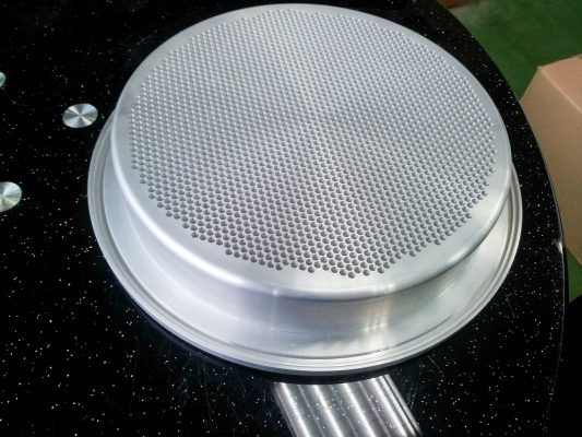
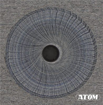
ATOM micro-drilling on Shower Head (aluminum alloy) processing effect
Although it looks like a shower head, the price of a Shower Head is as high as over 400,000 yuan. The fundamental reason for its high cost is the extremely stringent processing requirements - there are thousands of micro-holes on the surface, which not only imposes extremely high standards on the accuracy and consistency of the hole diameter, but also places almost stringent requirements on the smoothness and flawlessness of the inner wall of the hole.
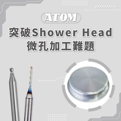
Shower Head, a business opportunity but with strict process requirements
According to Techcet's forecast, the global semiconductor Shower Head market size will be approximately US$2.5 billion in 2023, and is expected to grow to US$3.5 billion by 2028, with a compound annual growth rate (CAGR) of 6.9%. This is mainly due to the improvement of film deposition process requirements for advanced process chips (such as 3nm and below), and the demand for high-quality films due to the increase in the number of 3D NAND memory layers.
The most widely used metal material in Shower Head is aluminum alloy, because it has good thermal conductivity and strong corrosion resistance. Non-metallic Shower Head materials include silicon carbide (CVD-SIC), single crystal silicon, quartz glass and high-purity ceramics.
Aluminum alloy Shower Head
During the wafer reaction process, the surface of the gas diffusion plate is densely covered with micropores (pore diameter 0.2-6 mm). Special process gases need to pass through precisely designed pore structures and gas paths, and then be evenly deposited on the wafer surface after passing through thousands of small holes on the gas diffusion plate. The film layers in different areas of the wafer must ensure high uniformity and consistency.
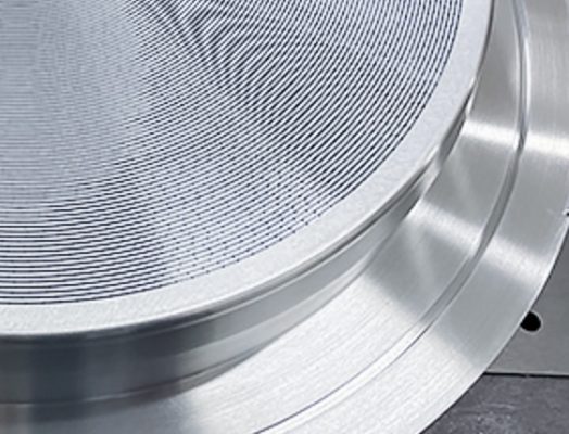
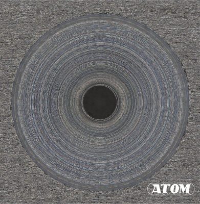
ATOM micro-drilling Shower Head processing effect (front and back)
Therefore, in addition to extremely high requirements for cleanliness and corrosion resistance, the gas diffusion plate also has strict requirements on the consistency of the aperture of the small holes and the burrs on the inner wall of the small holes. If the aperture size tolerance and consistency standard deviation are too large or there are burrs on any inner wall, it will cause the thickness of the deposited film layer to be inconsistent, which will directly affect the manufacturing yield of the equipment.
ATOM, the expert in micro-diameter drills, challenges the micro-hole processing problem with extreme precision
How to achieve the extreme micro-hole processing needs of Shower Head, a key component in the high-end semiconductor segment?
ATOM, the expert in micro-diameter drills in Japan, has launched two high-performance series of products specifically for the extreme micro-hole processing challenges such as Shower Head (aluminum alloy), helping semiconductor-related fields to efficiently break through the micro-hole processing challenges!
1. Fixed-point guided drilling NC: precise positioning, starting from the "hole"
Designed for high-precision, small-diameter guide holes (positioning), suitable for applications with extremely high hole position accuracy requirements.
(1) Processing range Ø0.02mm~Ø3.0mm, meeting various micro-hole positioning needs.
(2) Two drill point angles of 120° and 90° are available, taking into account both precise positioning and chamfering.
(3) With 3.0mm and 3.175mm tool holders.
(4) Suitable for materials such as steel, PEEK engineering plastics, non-ferrous metals and resins.
(5) Fully one-piece molding of all-tungsten steel material, with TiAlN coating, HRA hardness of about 90, wear-resistant and stable.
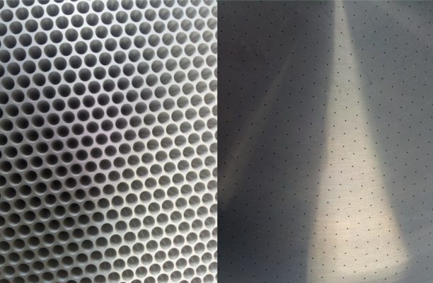
Without ATOM fixed-point drilling
Processing effect with ATOM fixed-point drilling
It can be clearly seen from the above figure that without using the ATOM-NC fixed-point drill, obvious surface vibration and concentricity deviation occurred in the processing of the 1.6mm diameter; while with the ATOM fixed-point drill, the situation was significantly improved. Although it is just a small pre-positioning step, it is directly related to the stability and accuracy of subsequent micro-hole processing. Ignoring it may even cause the entire workpiece to be scrapped, resulting in unnecessary losses.
2. Diamond-like coating drill bit DLC: wear-resistant blade protection, improved efficiency

(1) The DLC Shine Coating technology is used, which has ultra-high hardness (sp³ value up to 60GPa), significantly extending the tool life.
(2) The ultra-thin coating with low friction coefficient effectively prevents chip adhesion, reduces cutting resistance, and improves chip removal.
(3) The minimum diameter is Ø0.1 to Ø1.0, with a standard specification every Ø0.01mm.
(4) Suitable for non-ferrous metal materials such as aluminum alloy and copper.
ATOM can also customize center-drill heads. You only need to tell us the hole diameter, depth, and workpiece material, and we will provide you with the most suitable solution! When used in Shower Head processing, ATOM micro-drilling can greatly improve chip removal efficiency and significantly improve the roughness of the hole wall to achieve a smoother processing surface.
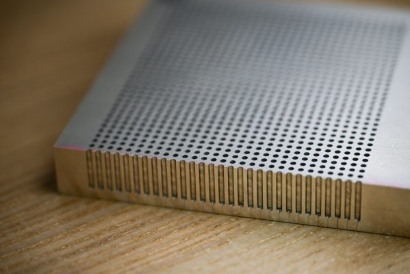
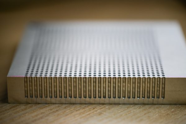
ATOM Micro-Drilling Shower Head Stage Hole Cross-Section
After repeated verification, the two series of ATOM can maintain extremely low tool wear even in large-scale micro-hole processing with their excellent wear resistance and ultra-long tool life, ensuring high consistency of micro-hole diameter and excellent surface finish, fully meeting the stringent requirements of aluminum alloy Shower Head for ultimate processing quality.
Learn more about drills :https://asun-photonics.com/product-category/atom/
ASP Group: Using world-class technology to help upgrade precision hole processing
ASP Group is the general agent of the Japanese ATOM brand in Taiwan, focusing on the promotion and service of high-quality micro-diameter tools. Relying on the strong manufacturing and quality control capabilities of the ATOM original factory, as well as ASP Group's advantages in logistics supply and technical support, it can now provide a rich product line including standard drills ADR, standard coated drills ADR-SV, fixed-point drills NC, chip removal drills ASWR/ASWD, diamond-like coated drills ADR-DLC, same-shank diameter drills ADS and cross-groove series drills SXG, etc., to fully meet various high-precision micro-hole processing needs and help customers achieve dual improvements in processing quality and efficiency.
1. Spot supply:
ASP Group has a rich stock of spot stocks, which can support the spot supply of ADR standard drill series and ADR-SV standard coated drill series Ø0.02mm~ Ø1.0mm (one standard specification for each Ø0.01mm).
2. High-efficiency delivery:
ASP Group has more than 20 years of experience in micro-hole processing technology services. It not only provides customers with professional demand analysis and application suggestions, but also relies on its strong supply chain advantages to help customers achieve spot delivery of standard drills within one week.
Contact Us
As semiconductor high-end manufacturing moves towards higher quality, the micro-hole processing quality of the Shower Head, as a key component, has become a key factor affecting the overall process yield.
ASP Group has teamed up with Japan's ATOM to use the ultimate micro-drilling technology to jointly provide the semiconductor industry with more stable and efficient micro-hole processing solutions. By continuously deepening the development of micro-diameter tool technology, it helps more advanced manufacturing scenarios achieve the leap from "machinability" to "excellent processing."