TRI's Inspection and Metrology Applications include: Chiplet & Chip-on-Wafer (CoW), System-in-Package (SiP), Advanced WLP, TSV Metrology, μBump, Cu Pillar, Surface Topology, Profiling, Thin Film Thickness, Patterned Wafer, Inner Crack / Chipping, After Sawing Defects, Die Underfill, Glue, Epoxy & Flux, Wafer Bumping and Die / Wire Bonding.
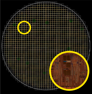 | 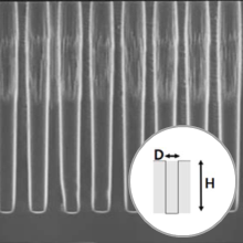 | 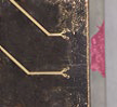 | 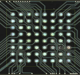 |  |
| Patterned Wafer | TSV Metrology | Wafer Frame | Wafer Bumping | Wire/Die |
 | |  | |  |
| SWIR+AI | | Chiplet Metrology | | Wafer AVI |