Loading...

Oxford Instruments

HsinChu County,  Taiwan
http://www.oxinst.com
  • Booth: I2022

Welcome to visit us at Booth I2926 to meet our experts!

Overview

Oxford Instruments plc is a leading provider of high technology products and services to the world's leading industrial companies and scientific research communities.

Our core purpose is to support our customers to address some of the world's most pressing challenges, enabling a greener economy, increased connectivity, improved health and leaps in scientific understanding.

Oxford has a broad spectrum of capability and expertise, composing of 8 business units structured into two divisions:

Materials and Characterisation develops products and solutions that enable the fabrication and characterisation of devices down to the atomic scale.

  • Asylum Research is the Technology Leading Manufacturer for Atomic Force Microscopy.
  • Magnetic Resonance is a leader in benchtop NMR spectroscopy and time domain (TD-NMR) relaxometry solutions enable novel research and optimise quality control.
  • NanoAnalysis provides leading-edge tools that enable materials characterisation and sample manipulation at the nanometre scale.
  • WITec is a leader in d Raman, Atomic Force Microscopy, and Scanning Near-field Optical Microscopy.

Research and Discovery provides advanced solutions that create unique environments and enable imaging and analytical measurements down to molecular and atomic levels:

  • Andor Technology are global leaders in the development and manufacture of high performance scientific digital cameras, microscopy systems and spectrographs for academic, industrial and government applications.
  • Imaris is the world’s leading Interactive Microscopy Image Analysis software company, actively shaping the way microscopic images are processed through constant innovation and a clear focus on 3D and 4D imaging.
  • Plasma Technology is a leading provider of etch & deposition processing equipment & solutions.
  • NanoScience are world leaders in dilution refrigerators and ultrahigh magnetic field environments for research applications including quantum technologies, nano technology research, advanced materials and nano device development.
  • X-Ray Technology is a leading manufacturer of x-ray tubes, power supplies, and integrated x-ray sources.

We are proud to be recognised as the leaders in what we do and for the difference we make in the world.


  Press Releases

  • Oxford Instruments, a leading provider of advanced plasma processing solutions for the compound semiconductor industry, today announced its role in supporting ROHM Co., Ltd. as the company transitions 650V gallium nitride (GaN) power device manufacturing in-house.

    By leveraging Oxford Instruments’ 200 mm GaN plasma atomic layer etch (ALE) technology, ROHM is implementing a proven process into its own high-volume manufacturing environment and scaling to 200 mm wafer size.

    This strategic move marks a major step in ROHM’s ambition to establish a fully integrated, end-to-end GaN production capability within the ROHM Group. GaN power devices offer significant advantages over traditional silicon technologies, including higher efficiency, faster switching speeds, and reduced system size. ROHM has already been supplying its EcoGaN™ series, which leverages these advantages to deliver high-efficiency, compact power solutions. The initiative will enable ROHM to strengthen supply capacity and meet rapidly growing demand for high-efficiency power devices across applications including electric vehicles (EVs), AI servers, and industrial power systems.

    Oxford Instruments’ industry-leading ALE technology with EtchpointTM, an exclusive collaboration with LayTec for real-time optical in-situ monitoring, allow GaN device manufacturers to control residual post-ALE layer thicknesses to an accuracy of +/-0.5 nm. These world-first integrated technologies are critical for ROHM to successfully bring the advanced process technology into its own fabs, delivering the state-of-the-art processing required to successfully replicate and scale advanced GaN device architectures.

    “What started out as a GaN R&D collaboration between ROHM and Oxford Instruments is expanding into the preparation for volume production ramp, and ROHM’s decision to bring GaN manufacturing in-house represents an important milestone for the power electronics industry,” said Matt Kelly, President, Oxford Instruments Advanced Technologies. “Our advanced etch solutions are specifically designed to enable ultra-low damage etching, atomic-scale precision, high uniformity, and repeatability, for high-volume 200 mm production environments. We are proud to support ROHM as they build a robust, high-volume manufacturing platform in-house for next-generation GaN power technologies.”

    “We are pleased to strengthen our collaboration with Oxford Instruments, whose industry-leading ALE technology supports our efforts, as we advance our strategy to establish a fully integrated, in-house GaN production platform. By bringing key manufacturing processes in-house, we aim to enhance control over technology and quality, strengthen our supply capabilities, and improve our competitiveness in the rapidly growing GaN market. This initiative will enable us to accelerate the delivery of high-efficiency power solutions for applications such as electric vehicles and AI infrastructure,” said Yasushi Hamazawa, Executive Officer, ROHM Co., Ltd. “We will continue to advance our GaN technologies to deliver higher performance and contribute to improved energy efficiency.”
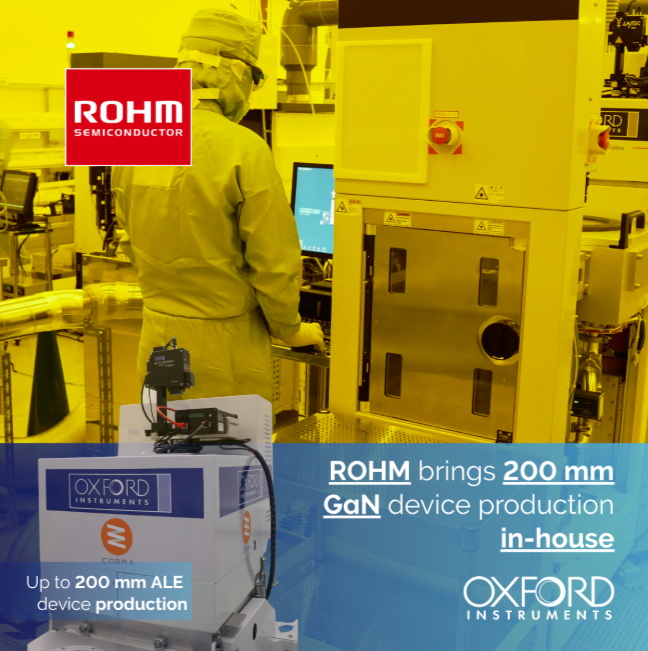
    ROHM brings 200 mm GaN device production in-house.

  • Oxford Instruments provides Coherent with state-of-the-art, fully automated processing equipment for 6” InP wafer processing, enabling next-generation AI applications.

    Oxford Instruments (OXIG), a leading provider of advanced plasma processing solutions for the compound semiconductor industry, announces the key role it is playing to support the industry’s first fully automated 6-inch indium phosphide (InP) wafer fabrication capability for photonic devices, led by Coherent Corp. (NYSE: COHR), a global leader in compound semiconductors and high-performance optical networking solutions.

    Oxford Instruments’ cutting-edge plasma processing equipment is central to Coherent’s groundbreaking achievement of ramping up 6-inch InP fabs in Sherman, Texas, and Järfälla, Sweden. These fabs will play a pivotal role in driving advancements in AI datacentre, telecommunications, and sensing applications. Coherent’s transition to 6-inch wafers is set to deliver significant benefits, including a substantial increase in capacity, lower die cost and more than four times the number of devices per wafer.

    Oxford Instruments has supplied fully automated, high-throughput 6-inch InP processing equipment, enabling Coherent to achieve these remarkable productivity gains. This advanced equipment is designed to support the transition from 800G to 1.6T products, a key requirement to meet the growing demands of AI interconnects and optical communications.

    “We have been the leading supplier of InP plasma etch equipment to the datacom market, and Coherent, for many years. Our technology, with the quality, throughput and reliability that we have developed alongside excellent service, is ideally positioned to support the current device demand inflection we are seeing with the release of generative AI applications. We are delighted to be partnering with Coherent during this exciting period of market expansion and look forward to continuing to develop and release innovative and valuable plasma processing solutions.” Matt Kelly, Managing Director, Oxford Instruments Plasma Technology.

    "Coherent’s move to 6-inch InP wafer fabrication marks a transformative milestone for the industry. Oxford Instruments’ expertise in plasma processing has been essential in enabling our Sherman and Järfälla fabs to reach world-class performance,” said Dr. Beck Mason, Executive Vice President – Semiconductor Devices at Coherent. “Together, we are advancing InP technology to support faster networks, greater efficiency, and the new applications that will define the future of connectivity."

    The joint efforts of Oxford Instruments and Coherent have culminated in a manufacturing platform that sets the stage for the next generation of InP optoelectronic devices. These devices are critical enablers for applications ranging from AI datacentres and datacom transceivers to advanced sensing in consumer electronics and automotive technologies.

  • We’re excited to bring you Semi Interface Issue #5: Opto datacom Edition, where we explore the innovations and collaborations shaping the future of technology. In this edition, we highlight the exciting breakthroughs that are advancing AI, AR wearables, silicon photonics, and more—pushing the boundaries of connectivity, datacentres, and intelligent machines.

    At Oxford Instruments, we are privileged to work alongside industry leaders and researchers to tackle some of the most complex challenges in semiconductor manufacturing. Working with Coherent and AOI, we are at the leading-edge of indium phosphide (InP) technology, including 6-inch wafer processing. Our collaboration with Quantemol on tailored waveform biasing (TWB) could enable next-generation fabrication capability, which is an exciting development in plasma innovation.

    We also shine a spotlight on our new state-of-the-art technical training suite in Bristol, UK, designed to empower our customers with the skills and knowledge to optimise system performance and operational efficiency. Join us as we share these stories and more, highlighting our service strategy, people, technologies, and partnerships driving industry transformation.

    Download the magazine here!

  • We’re excited to bring you Semi Interface Issue #4: WBG Power Edition, where we explore the transformative potential of silicon carbide (SiC) and gallium nitride (GaN) in reshaping power and RF electronics. This edition brings together insights from leading global experts, showcasing advancements in plasma technologies for interface optimisation and nitride ALD innovations driving volume manufacturing and reliability. We also highlight SiC’s emerging role in augmented reality, enabling immersive user experiences with exceptional clarity, durability and comfort.

    This issue features collaborative innovations, such as the co-development work between the University of Warwick and Oxford Instruments on trench etch & fill, and atomic scale processes presented at ICSCRM 2025 in Busan, South Korea. We also report on Singapore’s advancements, including insights from SEMICON Southeast Asia and Oxford Instruments’ involvement in the Singapore NSTIC GaN initiative. Additionally, expert voices from industry leaders provide perspectives on atomic-scale plasma processing, with a particular focus on South Korea’s developments.

    Packed with cutting-edge technology and global perspectives, Semi Interface Issue #4 highlights how SiC and GaN are evolving into strategic technology platforms, transforming industries and enabling the next generation of innovative applications.

    Download the magazine here!

  • Welcome to the second issue of Semi Interface magazine. We are once again joined by technology experts from around the globe, who in this issue share fascinating insights into the world of optoelectronics and datacoms.

    Our authors dive into the current monumental changes that the datacom market is experiencing and discuss the tech advancements needed to keep up with exponentially increasing demand for data transceiving devices. Datacom, microLEDs, augmented reality, and more market and technology expertise is shared in this magazine, and you can get your FREE COPY below.


  Products

  • Atomfab ALD
    High-throughput Atomic Layer Deposition (ALD) system designed for large-scale manufacturing of advanced semiconductor devices, including GaN power devices. Known for exceptional uniformity, conformality, and low cost per wafer....

  • High-throughput Atomic Layer Deposition (ALD) system designed for large-scale manufacturing of advanced semiconductor devices, including GaN power devices. Known for exceptional uniformity, conformality, and low cost per wafer.
  • PlasmaPro 100
    Versatile plasma etch, deposition, and ALE platform offering a variety of plasma processes for high-volume device manufacturing for InP/GaAs optoelectronics, GaN/SiC power devices, as well as processes for microLED, sensors and MEMS....

  • Versatile plasma etch, deposition, and ALE platform offering a variety of plasma processes for high-volume device manufacturing for InP/GaAs optoelectronics, GaN/SiC power devices, as well as processes for microLED, sensors and MEMS. Offers excellent process control and uniformity for consistent results.
  • Ionbeam
    Our ion beam etch (IBE) is a popular choice for high-quality slanted and blazed grating etch & ion beam deposition (IBD) processes. Flexible hardware options include open load, single-substrate load lock, and cassette-to-cassette configurations....

  • Our ion beam etch (IBE) is a popular choice for high-quality slanted and blazed grating etch & ion beam deposition (IBD) processes. Flexible hardware options include open load, single-substrate load lock, and cassette-to-cassette configurations. Specifications are tailored to each application, enabling faster, repeatable process results.
  • Ultim Extreme Infinity (EDS)
    Energy Dispersive Spectroscopy (EDS) systems known for their superior resolution, speed, and reliability, enabling rapid elemental analysis and mapping for process monitoring, quality control, and failure analysis in semiconductor devices....

  • Energy Dispersive Spectroscopy (EDS) systems known for their superior resolution, speed, and reliability, enabling rapid elemental analysis and mapping for process monitoring, quality control, and failure analysis in semiconductor devices.
  • Symmetry S3 (EBSD)
    A fast and accurate Electron Backscatter Diffraction (EBSD) system for high resolution analysis of grain structure, crystal orientation, and strain....

  • A fast and accurate Electron Backscatter Diffraction (EBSD) system for high resolution analysis of grain structure, crystal orientation, and strain.
  • WITec alpha300 Raman Microscopes
    Enable non-destructive, label-free chemical characterisation with high spectral and spatial resolution, offering comprehensive analysis for diverse materials and life science applications without sample preparation....

  • Enable non-destructive, label-free chemical characterisation with high spectral and spatial resolution, offering comprehensive analysis for diverse materials and life science applications without sample preparation.

Send Email

Type your information and click "Send Email" to send an email to this exhibitor. To return to the previous screen without saving, click "Reset".