Loading...

Accretech America Inc.

Fremont,  CA 
United States
https://www.accretech.com/en/
  • Booth: 1241

Visit Accretech America Inc. at Booth #1241!

Overview

ACCRETECH is a leading global provider of advanced semiconductor manufacturing equipment. With a focus on precision, innovation, and reliability since 1949, ACCRETECH delivers cutting-edge solutions for wafer probing, dicing, and process control, supporting the evolving needs of semiconductor manufacturers worldwide. Guided by the philosophy of “Growing Together with Partners,” ACCRETECH works closely with customers to enhance productivity, performance, and technological advancement across the semiconductor industry.

Visit www.accretech.com to discover how our products are shaping the future of the semiconductor industry.


  Press Releases

  • Nagoya Plant

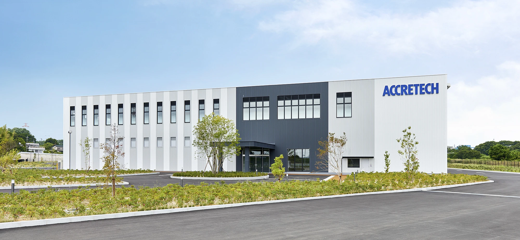
    TOKYO SEIMITSU CO., LTD. (the Company; Head Office: Hachioji-shi, Tokyo; President and CEO: Ryuichi Kimura) has completed construction of the new Nagoya Plant, which was being built by its subsidiary Tosei Engineering Corp., as part of its efforts to further expand its semiconductor manufacturing equipment business. The completion ceremony was held on August 27, 2025.

    Background and purpose of the new plant

    In recent years, with the expansion of communication technologies such as AI, IoT, and cloud computing, the demand for semiconductors and electronic components has been increasing year by year. As a result, the demand for semiconductor production equipment (SPE) provided by the Company has grown significantly from semiconductor device manufacturers and electronic component manufacturers, and there is also an increasing demand for new SPE to produce high-performance devices.

    In this context, grinding technology tailored to specific applications is essential for achieving the high performance of semiconductor devices, particularly in areas such as 3D packaging (advanced packaging) and compound semiconductor processing. As a result, demand for the grinders the Company manufactures and sells continues to grow.

    Furthermore, in recent years, a technology called “hybrid bonding” has been proposed, which enables high-density packaging by precisely stacking and bonding multiple semiconductor chips or wafers. This process is expected to play a crucial role in the development and mass production of next-generation semiconductor devices. In this process, high-precision grinding processes that “thin and uniformly reduce the thickness of wafers and ensure flatness for bonding” are indispensable, and grinders with even higher precision than before are now in demand.

    In response to this market environment, the Company has determined that securing production capacity for grinders for hybrid bonding, which are expected to present significant mid- to long-term business opportunities, is an urgent priority for establishing a stable production and supply system for grinders.

    The completed new Nagoya Plant is primarily dedicated to the production of grinders for hybrid bonding, while also manufacturing other back grinders for silicon wafers. This expansion is expected to approximately double the Tokyo Seimitsu Group’s grinder production capacity compared to previous levels.

    Tokyo Seimitsu Co., Ltd. will continue to support its global customers' manufacturing operations with an even stronger and more robust business structure.

    Establishment of Chubu Metrology Center

    The Company is also pleased to announce the establishment of Chubu Metrology Center within new Nagoya Plant as a facility dedicated to deepening understanding of precision measurement technology. This center will serve as a hub for providing technical support and solutions tailored to the needs of the Chubu region, which is a major manufacturing hub in Japan. Through this initiative, the Company will further enhance its ability to address its customers' measurement challenges with tailored proposals and solutions.

    The center features a wide range of products, including coordinate measuring machines, non-contact contour measuring instruments, and surface texture measuring instruments, all of which are on display. The Company has created an environment where it provides customers with measurement evaluation, equipment operation, and solution proposals with one-stop.

    Furthermore, the Company plans to collaborate with local educational institutions and local companies to host study sessions and facility tours, thereby fulfilling the role of an educational hub for precision measurement.

    Outline of the new Nagoya Plant

    Name Tosei Engineering Corp. Nagoya Plant
    Address Togo-cho, Aichi-gun, Aichi Prefecture
    Building description 2 floors above ground (steel structure)
    Total site area 35,887.68m2
    Total floor area 13,134.82m2
    Main production item Grinders, Wafer Demounting and Cleaning Machines, Dedicated Measuring Machines
    Start of operation From August 27, 2025 onwards

  Products

  • AP3000 Wafer Probing Machine
    AP3000/AP3000e is a next-generation ultra-high-performance probing machine designed to achieve high precision, high throughput (index move, wafer handling, and wafer alignment), low vibration and low noise....

  • The AP3000/AP3000e is a next-generation ultra-high-performance probing machine designed to achieve high precision, high throughput (index move, wafer handling, and wafer alignment), low vibration and low noise.
    Anti-Virus/Anti-Malware software is installed as standard software on the machine.
    The functions and operability of AP3000/AP3000e are inherited from previous models, and it maintains compatibility of recipe and map data. It is very user friendly with safety and security in mind.

    Features:


    Needle cleaning (cleaning wafer, or cleaning unit)

    Fan filter unit (mini-environment)

    HF jig/manipulator, Tester interface

    Loader : 2 Loader / Automation with AMHS

    Head stage tilt (Probe card tilt)

    Chuck: Ambient / Hot temp. / Low temp. /Low noise

    APC : Auto probe card exchange

    Cassette ID reading

    Wafer ID reading (Top surface / Back surface)

    GB-IB Interface

    Prober Network (Veganet, Light-Veganet, Vega-Planet, GEM)

    PCAS (Probe card auto setup)

    Probe card PGV

    PLP testing for up to 300mm square

  • SS20 Dicing Machine
    Semi-automatic dicing machine for Φ200mm wafers...

  • The same high rigidity and gate type structure as in the fully automatic dicer are used. A stable cutting environment is provided by using a structure that is not easily affected by heat contraction or vibration. The maximum workpiece size is Φ 200mm, and the square table specification can handle up to 250 mm square substrates. The use of our originally developed axial mechanism contributes to the speeding up of the X, Y, Z axes and the enhanced throughput. A 1.8 kW rating, high-output spindle is equipped as standard. A broad range of uses from silicon to electronic devices can be supported.

    Features

    Compact design, φ200mm wafer compatible dicing machine
    A wide range of materials are supported, from silicon to difficult-to-cut materials. 
    When the square table is selected from the special specification, processing of substrates up to 250mm2 can also be supported. 


    High-performance, high-output spindle equipped as standard
    1.8 kW rating, maximum rotation speed of 60 krpm (a 2.2 kW rating high-torque spindle can also be equipped as an option)


    Enhanced productivity (throughput) 
    Increased rigidity + servomotorization of the X, Y, Z axes
    Establishment of both a reduced footprint and high throughput


    High scalability (the standard specification supports various processing modes)
    The feature with multiple workpiece support and an alignment corresponding to the state with multiple workpieces applied to 1 tape frame, and the feature in which the workpiece distortion is detected by the alignment treatment, and the cutting position (Y, θ) is corrected so that the optimal chip is obtained, etc., are equipped as standard. 
    Software features required for various processing uses are equipped as standard, and a wide range are supported from silicon to electronic component processing. 

    Operability
    A 17-inch touch panel + GUI (Graphical User Interface) are used. 
    Simply by touching the iconized buttons, straightforward and comfortable operation is achieved. 
    The device is equipped with an operation system in common with the AD/SS Series whose use is familiar.

    Specifications

    Maximum work size Φ 200 mm, □ 250 mm
    Spindle Number of rotations 60,000 rpm
    Maximum blade diameter Φ 2 to 3 inch (Φ 60 to 80 mm)
    Rating output 1.8 kW
    X axis Cuttable range 260 mm
    Fastest speed 800 mm/sec
    Y axis Cuttable range 260 mm
    Fastest speed 300 mm/sec
    Cumulative precision 0.002 mm/260mm
    Z axis Stroke 35 mm
    Fastest speed 80 mm/sec
    Repeatability 0.001 mm
    Θ axis Rotation range 380°
    Specifications Voltage 3 Phase AC200 to 220 V ±10 %
    (Other than the above, compatible with a transformer)
    Consumed electric power 4.0 kVA(MAX)
    Air supply pressure 0.55 to 0.7 MPa
    Average consumed volume of air 180 L/min (at 0.55 MPa)
    Cutting water, other (pressure) 0.3 to 0.5 MPa
    Cutting water, other (maximum flow rate) 2.0 L/min
    Cooling water (pressure) 0.3 to 0.5 MPa
    Cooling water (maximum flow rate) 1.9 L/min (at 0.3 MPa)
    Exhaust flow rate 5 ㎥/min or more
    Dimensions (W x D x H) 890 mm×1,000 mm×1,560 mm
    Weight 792kg


Send Email

Type your information and click "Send Email" to send an email to this exhibitor. To return to the previous screen without saving, click "Reset".