Loading...

Ushio, Inc.

  • Booth: 1435

For litho, surface treatment, or heating, visit USHIO now!

Overview

Established in 1964, USHIO INC. (TOKYO: 6925) is a leading manufacturer of light sources such as lamps, lasers, and LEDs, in a broad range from ultraviolet to visible to infrared rays, as well as optical equipment that incorporate these light sources. 

USHIO exhibits the following products:

  • UX-series photolithography systems
  • Excimer 172nm UV surface treatment systems
  • Halogen lamps for heating process of semiconductor
  • Flash lamp annealing equipment
  • LED annealing equipment


  Press Releases

  • 2025.08.05

    Ushio Inc. (Head office: Tokyo, President and CEO: Takabumi Asahi, hereinafter "Ushio") hereby announces that the development outlook for the UX-59113, a stepper for advanced packaging that achieves a resolution of L/S=1.5μm and an exposure field of 100mm square or more per shot, has been established, and plans to launch this product within fiscal year 2026.

    The UX-5 series is a lithography equipment for cutting-edge IC package substrates, boasting a 90% global market share*, and is used to expose semiconductor package substrates built into a variety of devices, including PCs, smartphones, and tablet devices.

    The spread of IoT and the emergence of generative AI is driving increased demand for high-performance semiconductors for data centers. Advanced packages such as chiplets are seeing increasingly miniaturized interconnects and larger package sizes, driving market needs for alternatives to silicon interposers and full panelization. This is expected to drive increased demand for panel-level packaging using resin and glass substrates.

    With conventional steppers for wafer, larger package substrates require stitching, which involves connecting multiple shots for exposure, but misalignment during stitching can lead to issues with reduced yield and productivity. This product enables single-shot, stitchless exposure of substrates 100mm square or larger at 1.5μm resolution, improving yield and productivity during mass production.

    It addresses the critical issues of warping and undulation that commonly occur during mass production of glass substrates and full-panel size substrates, which are gaining attention as next-generation technologies. Its new platform leverages the advanced handling technologies we have developed through extensive experience with semiconductor package substrates to effectively solve these challenges.

    Ushio will advance the functionality of steppers for advanced package substrates to the world's highest level by leveraging the unique optical design technology it has cultivated since its founding and the know-how it has accumulated over many years working with customers in the IC package substrate industry.

    *Cutting-edge IC package substrate market (Stepper market)

    ■Main Features
    ・Single-shot exposure of substrates 100mm square or larger at 1.5μm resolution
    ・Light source and other components designed and incorporated into the equipment in-house
    ・Transport platform compatible with full-panel-size organic and glass substrates

    ■Appearance


    *Appearance and specifications are subject to change without prior notice.

    ■Ushio's lithography equipment lineup
    Aiming to expand and grow its advanced packaging business, in addition to conventional steppers and maskless direct imaging exposure systems, in December 2023, the company added a new product, the "DLT system," to its lineup through a business partnership with Applied Materials, Inc. This allows Ushio to steadily build a full lineup that meets the diverse needs of customers for next-generation packaging substrates, where technological innovation is advancing.

    With the addition of the new stepper product "UX-59113," which is compatible with interposer substrates that play an important role in advanced packaging, to the stepper lineup, we are able to build a comprehensive product lineup that meets a wider range of customer needs and contributes to technological innovation in next-generation package substrates, particularly for generative AI semiconductors.

    As a leading company in lithography equipment for cutting-edge IC package substrates, Ushio will continue to contribute to the realization of a convenient and comfortable society through its "light" technology.

    Product Portfolio (Image)


  • Ushio Inc. (Head office: Tokyo, President and CEO: Takabumi Asahi, hereafter "Ushio") has successfully developed new interference lithography equipment that achieves an interference fringe pitch accuracy of 0.01nm and realizes the formation of phase shift structures. The product is scheduled to be launched in the spring of 2027.

    The amount of power handled in data centers is becoming an issue due to increased competition in generative AI (Artificial Intelligence), and there are high expectations for photoelectronic fusion*. Laser light sources used for photoelectronic fusion are called DFB-Laser diodes (distributed feedback lasers) with diffraction gratings in the waveguide, and demand is growing rapidly. However, the productivity of EB (electron beam lithography) equipment used to form diffraction gratings is low and supply has not kept pace. It is widely known that interference exposure technology has the potential to solve the low productivity of EB, but has not yet been applied to mass production due to the following three issues.

    (1) Unable to obtain stable exposure quality
    (2) Low pitch accuracy
    (3) Phase shift structure cannot be formed


    This time, Ushio proposes a new interference lithography equipment that solves the above three issues.

    (1) Excellent exposure stability with DPSS laser and KrF photoresist
    Conventional interference lithography equipment uses a gas laser as the light source and a photoresist having strong linear property, resulting in a problem of low exposure stability. Ushio's interference lithography equipment uses a 266nm DPSS (Diode Pumped Solid State) laser as the light source and a chemically amplified KrF photoresist as the photoresist to achieve excellent exposure stability while maintaining exposure performance. (Figure 1)

    (a) SEM image (180 nm pitch)                                      (b) Capable of exposing the entire surface of an 8-inch wafer

    Figure 1: Experimental data

    (2) Pitch accuracy of 0.01nm achieved with our unique adaptive optical metrology
    Ushio's interference lithography equipment can directly measure interference fringes for exposure with an accuracy of 0.01nm. It also has an adaptive optical metrology to compensate for misalignment with the aiming pitch. This feature makes it possible to achieve the high pitch accuracy required for DFB laser diffraction gratings. (Figure 2)
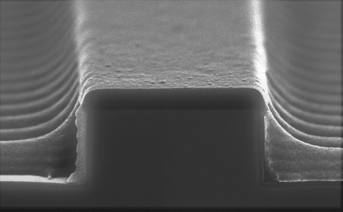

    Figure 2: Example of application to DFB laser (SEM image of patterning on a waveguide)

    (3) Formation of phase shift structures in combination with digital holographic elements
    The phase shift layer is known to improve yield by giving a discontinuous shape to a part of the diffraction grating. Ushio's interference lithography equipment uses a highly controlled digital holographic element to realize a CPM (Corrugation Pitch Modulation) structure with functions equivalent to those of a conventional phase shift layer. 

    Prior to the product launch, we are widely accepting orders for demonstration processing. This equipment has great applicability not only for Semiconductor Laser Diode (LD), but also for manufacturing optical components needed in AR (Augmented Reality).

    Ushio will continue to realize technological innovation in the Industrial Process area with "Light."

    The details of this technology will be presented at the IEICE Society Conference (Okayama University) scheduled for September 8th to 12th.

    * Technology that integrates electronic circuits handling electrical signals and light circuits handling light signals to replace electricity with light for data processing and communication, aiming for higher speed, lower power consumption, and higher capacity.

    ■3D-CAD drawing
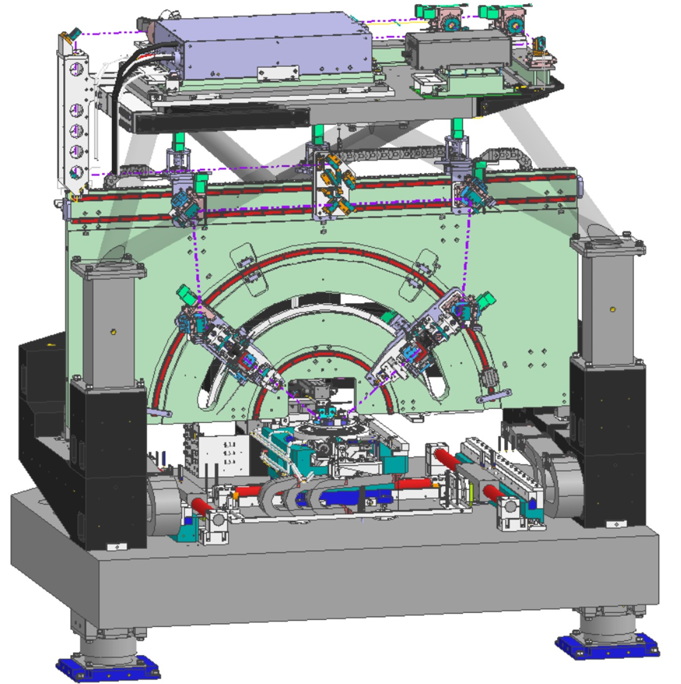


    ■Outline of equipment specifications
    Substrate size 8 inches or less
    Substrate thickness 2mm or less
    Resolution 150nm to 650nm
    Shot size 13.8 x 13.8mm and 22 x 23mm under development
    Alignment accuracy 1μm
    Transfer type Cassette-to-cassette transfer
    Throughput Approx. 5 wph for 6 inch wafer (depends on exposure method)
    Footprint 2.5 × 4m
    Substrate material Silicon, glass, compound semiconductors, ceramic materials in general, and other adsorbable materials
    Exposable patterns Line-and-space pattern, dot pattern
    Duty control Possible by adjusting exposure (0.3 to 0.55), depending on resist type
    *Appearance and specifications are subject to change without notice.

  Products

  • 172-nm Excimer Irradiation Unit
    Organic cleaning and surface reformulation are performed using 172-nm UV and radicals generated by itself. Surface reformulation can be performed without roughening the substrate surface, which contributes to improved adhesion of various materials....

  • Excimer Irradiation Unit 

    The world's highest irradiance and maximum exposure for unparalleled productivity! 

     Organic cleaning and surface reformulation are performed using vacuum ultraviolet light and radicals generated by itself.

    Surface reformulation can be performed without roughening the substrate surface, which contributes to improved adhesion of various materials.

  • Large-Area Projection Lithography Tool: UX-4, UX-5
    The lithography tools utilize Ushio's robust lighting and optical technologies, along with unique large-area projection lens technology....

  • Non-contact and large shot-size, capable of high productivity.   

    The lithography tools utilize Ushio's robust lighting and optical technologies, along with unique large-area projection lens technology.

    ・The UX-4 is capable of processing up to 8-inch wafers with non-contact and one shot per wafer. Enabling exposure on warped wafers using a greater depth of focus, which achieves higher productivity and better yield than proximity aligners.

    ・The UX-5 is designed as a stepper projection lithography tool for advanced packaging substrates, which is capable of exposing full-size (510x515mm) substrates. On August 5, 2025, Ushio announced the development outlook of the UX-59113 on top of our existing product line, a stepper for advanced packaging that achieves a resolution of L/S=1.5µm and exposure field of 100mm squared or more per shot. Please visit our booth and get in touch with our staff for more details.

    【Key Technologies】 

    • Equipped with the world's leading high-pressure UV lamp
    • Unique illumination optical system boasting high uniformity
    • Outstanding large-area projection lens
    • Large depth of focus for stable patterning
    • Large shot enables high productivity
  • Flash Lamp Annealer
    This is an annealing (light heating and light sintering) device using a flashlamp. It can instantaneously heat large areas (up to 500×500mm) with high output....

  • Ultra-short time annealing with high-power, wide-area irradiation, and precise control over the depth of heating in the target material.

    This is an annealing (light heating and light sintering) device using a flashlamp. It can instantaneously heat large areas (up to 500×500mm) with high output. Compared to conventional electric furnaces and halogen lamp heating furnaces, it boasts high-precision temperature control along the depth direction of the workpiece.

    The emitted spectrum ranges from ultraviolet to infrared, allowing for heating of various materials with absorption characteristics in that range.

    In particular, if you are facing difficulties in temperature control during the heating process, it may be the optimal solution for you.


Send Email

Type your information and click "Send Email" to send an email to this exhibitor. To return to the previous screen without saving, click "Reset".