Loading...

Nikon Precision

Belmont,  CA 
United States
https://www.nikonprecision.com
  • Booth: 6045

Visit Nikon Precision Inc. at SEMICON West, Booth #6045!

Overview

Since 1980, Nikon Corporation has been revolutionizing lithography with innovative products and technologies. The company is a worldwide leader in semiconductor lithography solutions for the microelectronics manufacturing industry with more than 8,000 (semiconductor) lithography systems installed worldwide. Nikon offers the most comprehensive selection of production-class steppers and scanners in the industry. These products serve the semiconductor, FPD, LCD, OLED and TFH industries. The extensive Nikon product portfolio includes specialized lithography solutions for MEMS, LED, and packaging applications as well. In addition, Nikon offers advanced semiconductor inspection systems. Nikon Precision Inc. provides service, training, applications and technical support, as well as sales and marketing for Nikon lithography systems in North America. For more information about Nikon, access our website at https://www.nikonprecision.com.


  Press Releases

  • Nikon’s first semiconductor lithography system for packaging applications

    Digital Lithography System
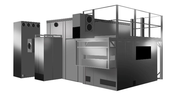
    Image of Digital Lithography System

    Tokyo, Japan – October 22, 2024 – Nikon Corporation (Nikon) is developing a digital lithography system with resolution of one micron (L/S) and high productivity for advanced semiconductor packaging applications. This product is scheduled to be released in Nikon’s fiscal year 2026.

    The rapid adoption of artificial intelligence (AI) technology is driving demand for integrated circuits (ICs) for data centers. In the field of advanced packaging, including chiplets, the size of packages is increasing with the miniaturization of wiring patterns. This will lead to heightened demand for panel level packages that use glass and other materials suitable for larger packages, requiring exposure equipment that combines high resolution with a large exposure area. To meet these demands, Nikon is developing digital exposure equipment that combines the high-resolution technology of its semiconductor lithography systems, which has been cultivated over many decades, along with the excellent productivity made possible with the multi-lens technology*2 of its FPD lithography systems.

    The digital lithography system does not use photomasks. Instead, it irradiates light from a source onto a spatial light modulator (SLM) that displays a circuit pattern and transfers it onto a substrate using a projection optical system. Since there is no need to design or produce photomasks, the digital lithography system also contributes to reducing costs, as well as shortening product development and manufacturing times.

    Nikon will continue to contribute to advanced semiconductor manufacturing by providing lithography systems and solutions to fully satisfy our customers’ goals and production requirements.

    *1 Abbreviation for Line and Space. Refers to the width of the wiring and the space between the adjacent wiring.

    *2 Nikon’s proprietary technology that exposes multiple projection lenses in an array and precisely controls them to produce the same effect as if a single giant lens were used. This enables patterning over a wider area with a single exposure.

    The information contained in this press release is current as of its date of publication.

    About Nikon
    Since 1980, Nikon Corporation has been revolutionizing lithography with innovative products and technologies. The company is a worldwide leader in semiconductor lithography systems for the microelectronics manufacturing industry with more than 8,000 (semiconductor) lithography systems installed worldwide. Nikon offers the most extensive selection of production-class steppers and scanners in the industry. These products serve the semiconductor, flat panel display (FPD) and thin-film magnetic head (TFH) industries. Nikon Precision Inc. provides service, training, applications and technical support, as well as sales and marketing for Nikon lithography equipment in North America. For more information about Nikon, access our website at https://www.nikonprecision.com.

    ####

    This press release contains forward-looking statements as that term is defined in the Private Securities Reform Act of 1995, which are subject to known and unknown risks and uncertainties that could cause actual results to differ materially from those expressed or implied by such statements. Such statements are subject to risks, uncertainties and changes in condition, particularly those related to industry requirements and other risks. The Company undertakes no obligation to update the information in this press release.

    For further information, please contact:
    Nikon Precision Marketing Communications at:
    [email protected]


  Products

  • Litho Booster
    Litho Booster Standalone Alignment Station maximizes productivity and yield. It delivers industry-leading shot-by-shot feed forward corrections for any selected scanner in the fab...

  • The Litho Booster Standalone Alignment Station brings inline Alignment Station (iAS) capabilities to other scanners in the fab. With Litho Booster, shot-by-shot feed forward correction is possible, enabling compensation for processing effects including etching, annealing, CVD/PVD, and more. Whereas traditional process loops rely on feed back control, Litho Booster adds sophisticated feed forward correction capabilities. Litho Booster quickly executes super dense, ultra-precise measurements with superior reliability, and calculates high order and die-by-die grid term as well as shot term corrections. Prior to exposure, the scanner performs wafer global alignment using a sparse EGA sampling plan, and the high order Litho Booster correction terms are fed forward and combined with the scanner’s linear terms to produce the final linear, high order grid, and shot term alignment corrections.

  • Nikon NSR-S636E ArF Immersion Scanner
    The S636E delivers world-class device patterning and productivity for diverse cutting-edge semiconductor manufacturing processes...

  • The NSR-S636E ArF immersion scanner is integrated with the inline Alignment Station (iAS) and incorporates the latest technology advances. The S636E delivers world-class device patterning and productivity for diverse cutting-edge semiconductor manufacturing processes. With the highest productivity of any lithography system across the impressive history of Nikon, the NSR-S636E is an immersion lithography scanner for critical layers that delivers superior overlay accuracy and ultra-high throughput. The NSR-S636E is the optimum patterning solution for the many diverse structures used in cutting-edge semiconductors, including 3D devices.

  • NSR-2205iL1
    The NSR-2205iL1 5x Reduction i-Line Stepper supports a variety of semiconductor devices and integrates well with existing fab equipment and operations...

  • The NSR-2205iL1 5x Reduction i-Line Stepper supports a variety of semiconductor devices and integrates well with existing fab equipment and operations. The NSR-2205iL1 leverages well-established Nikon technologies to deliver high stepper productivity with maximized yield across varying manufacturing processes. This includes high-accuracy wafer measurement using multipoint autofocus (AF), advanced wafer stage leveling*1, and large depth of focus (DOF) to maximize process window, among other central benefits. The 2205iL1 also accommodates a multitude of applications through compatibility with different wafer sizes and thicknesses, has high wafer warpage tolerance, and supports customers’ varied production applications including SiC (silicon carbide) and GaN (gallium nitride) processes.

    *1 Mechanism that corrects the shift between the exposure image plane and the substrate surface during exposure by tilting the platform (stage) on which the wafer is placed.

Categories


Send Email

Type your information and click "Send Email" to send an email to this exhibitor. To return to the previous screen without saving, click "Reset".